INNOVATION




Chip Semiconductor
Breakthrough in TGV Technology
SignificantProgress




TGV Technology – Breakthrough Progress
In the post-Moore era, semiconductor processes are approaching physical limits, and 2.5D/3D packaging is key to continuing Moore’s Law. The interposer layer, acting as a “bridge” for chips, plays a significant role. Traditional silicon-based interposers offer good performance but are costly (accounting for over 30% of packaging costs) and difficult to process; organic interposers are cheaper but have high-frequency losses and a high coefficient of thermal expansion, leading to significant warping, making them hard to meet high-density interconnect requirements. In contrast, glass-based interposers using TGV technology, with excellent RF performance, low expansion coefficient (good compatibility), high mechanical strength, and cost advantages, are set to become core materials for the next generation of advanced packaging. Although international giants have already made strides, domestic production has not yet achieved breakthroughs, but the potential in fields like HPC, AI, and 5G is enormous, and it is expected to become mainstream in high-end packaging, driving industry innovation.
Chip Semiconductor, leveraging its deep technical foundation in 2.5D packaging, continues to innovate. Recently, a breakthrough was achieved in the wafer-level Glass Interposer 2.5D fan-out packaging technology developed in collaboration with the Shitalong team from Southeast University, with all relevant technical indicators precisely meeting packaging design requirements. The first sample from this tape-out is a 2.5D integrated module aimed at AI acceleration chips, which includes one domestically produced GPU core using 7nm technology, four HBM2E memory chips with a single-chip bandwidth exceeding 460GB/s, and a 400μm thick Glass Interposer interconnect layer, providing robust hardware support for high-performance AI computing.
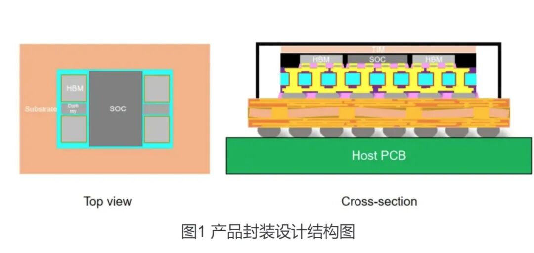
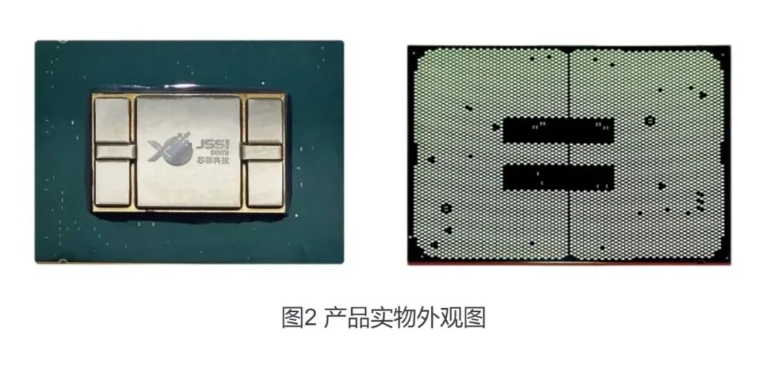
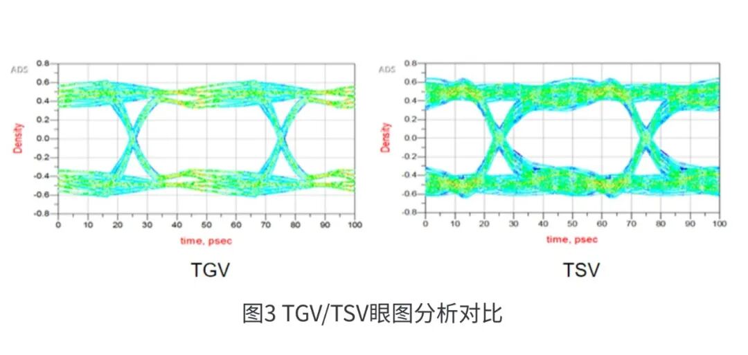
Simulation data shows: At the same frequency, the insertion loss of TGV interconnect structures is less than that of TSV; as the bit rate increases, the eye diagram indicators mostly deteriorate, yet TGV indicators still outperform TSV.
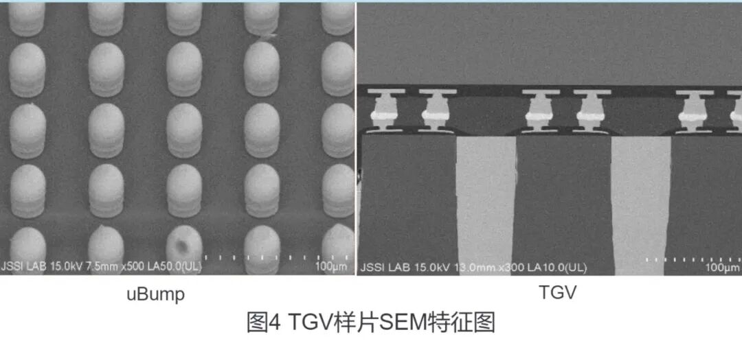
1. High-precision TGV (Through Glass Via) process: Achieving micro-hole processing with a diameter of 62.5μm and a depth-to-width ratio of 7:1, increasing interconnect density by three times;
2. Ultra-fine line RDL (Re-Distribution Layer): Line width/spacing ≤ 2μm, supporting high-density interconnect of 10⁴ I/O/mm², meeting HBM (High Bandwidth Memory) integration requirements;
3. Low warpage wafer-level packaging: Through material optimization and low-temperature bonding technology, controlling 300mm wafer warpage to <50μm, with a yield exceeding 97%;
4. RF performance optimization: Glass dielectric loss (Df) can be as low as 0.004@10GHz, also suitable for high-frequency applications such as 5G millimeter waves and optical communications.
Chip Semiconductor
Jiangsu Chip Semiconductor Technology Co., Ltd. was established in September 2020 and is an integrated circuit company based in Nanjing, dedicated to mid-to-high-end packaging and testing. Currently, it can provide customers with design and services for packaging products such as Bumping, WLCSP, Flip Chip PKG, QFN, BGA, SIP, SIP-LGA, and 2.5D.
The company adheres to a harmonious family-like culture, insists on a people-oriented approach, technological innovation, collective struggle, and professional management as its core values, and strives to fully meet customer needs as its greatest pursuit. Through continuous innovation and relentless hard work, it aims to develop advanced packaging and testing core technologies, making Chip Semiconductor a world-class packaging and testing enterprise, serving and promoting the development of the global semiconductor industry.
In March 2023, the Advanced Packaging Technology Research Institute of Chip Semiconductor launched the CAPiC platform, focusing on developing packaging technology centered on Chiplet heterogeneous integration, marking another breakthrough in advanced packaging technology, expected to drive heterogeneous integration to become mainstream in future chip design. For more information, please visit our official website https://www.jssisemi.cn/