Wafer foundry is the core segment of the semiconductor industry
Wafer foundry refers to the specialized manufacturing of semiconductor wafers, accepting orders from other integrated circuit (IC) design companies for production, without engaging in design. Wafer foundry is one of the important segments in the semiconductor industry, characterized by being technology-intensive, capital-intensive, and serving as a crucial link in the supply chain.
The business models of integrated circuit manufacturing companies mainly include IDM and wafer foundry models. Among them, wafer foundry refers to a semiconductor industry business model that accepts orders from fabless design companies, specializing in the processing of wafer products to manufacture integrated circuits, without engaging in product design and backend sales. This model arises from the specialization in the integrated circuit industry chain, forming a structure of fabless design companies, wafer foundry companies, and packaging and testing companies.
In wafer foundry, the foundry is responsible for the entire wafer manufacturing process, including procurement of raw materials, wafer growth, cutting, cleaning, thin film deposition, and subsequent packaging and testing steps, allowing chip design companies or brand owners to focus on key areas such as product design, marketing, and R&D, while entrusting the manufacturing process to specialized foundries. This can save a significant amount of funds and resources, reduce production costs and risks, and make them more flexible and agile in market competition. Therefore, after years of development, wafer foundry has become an indispensable core segment of the global semiconductor industry.
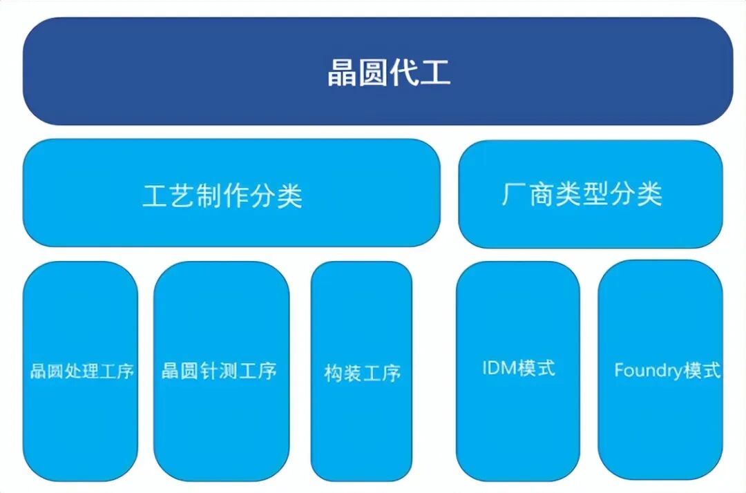
Classification of wafer foundry processes and types of manufacturers
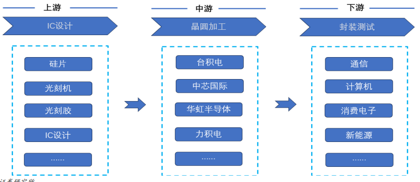
Wafer foundry is the core segment of the semiconductor industry. The upstream of the wafer foundry industry chain includes semiconductor materials, equipment, and related design service supply segments, mainly including silicon wafers, photoresists, masks, electronic special gases, sputtering targets, and other semiconductor materials, photolithography machines, etching machines, ion implantation machines, coating and developing equipment, thin film deposition equipment, and IC design services. The midstream wafer foundry processing service segment includes processes such as wafer cleaning, photolithography, etching, ion implantation, annealing, diffusion, chemical vapor deposition, and chemical mechanical polishing.
Representative wafer foundry companies in the market include TSMC, GlobalFoundries, SMIC, Hua Hong Group, World Advanced, Powerchip, and Jinghong Integrated. The downstream wafer packaging and testing segment, as well as the end application fields of consumer electronics, semiconductors, photovoltaic cells, and industrial electronics.
Wafer foundry industry chain
Development history of wafer foundry
1970s-1980s: The era of integrated design and manufacturing (IDM). In the early semiconductor industry (such as Intel, Texas Instruments, Motorola, IBM, etc.), the IDM (Integrated Device Manufacturer) model was implemented, where chip design, manufacturing, and packaging were all self-operated. At that time, manufacturing equipment was expensive, and the technical threshold was extremely high, making it difficult for small companies to enter the manufacturing sector. The chip industry was dominated by large companies.
Mid-1980s: The wafer foundry model was born. In 1987, TSMC (Taiwan Semiconductor Manufacturing Company) was founded by Morris Chang in Taiwan, pioneering the pure manufacturing, no-design wafer foundry business model. The wafer foundry model emerged for the first time, breaking the monopoly of IDM.
1990s: Wafer foundry took off as TSMC rapidly expanded production and improved process capabilities, becoming the world’s leading foundry. UMC (United Microelectronics Corporation) also transformed into a professional wafer foundry company in Taiwan. In the United States, Chartered Semiconductor (later merged into GlobalFoundries) emerged. The fabless company boom: more and more design companies emerged, driving explosive growth in mobile communications and consumer electronics. The “Fabless + Foundry” model became a new mainstream model.
2020s to present: Advanced processes, geopolitical factors, and global layout have entered the 3nm era, with TSMC, Samsung, and Intel (returning to the foundry market, establishing IFS) engaging in direct competition. Geopolitical tensions (the US-China tech war) have prompted wafer foundry capacity to begin global distribution (TSMC setting up factories in the US and Japan, Samsung investing in Texas, SMIC accelerating expansion in mainland China). Emerging fields (automotive electronics, AI chips, IoT) are presenting more segmented demands for wafer foundry. Mature processes (such as 28nm, 40nm) have also become key competitive areas, especially in automotive and industrial sectors.
Wafer foundry is classified into advanced processes and mature processes
With the continuous emergence of new demands in downstream application scenarios, the variety of semiconductor products is constantly increasing. To meet the differentiated demands for product functions and performance in the market, IDM manufacturers and wafer foundry companies involved in wafer manufacturing processes are continuously innovating wafer manufacturing process technologies, evolving into differentiated manufacturing processes. Wafer manufacturing processes can be roughly divided into advanced logic processes and specialty processes.
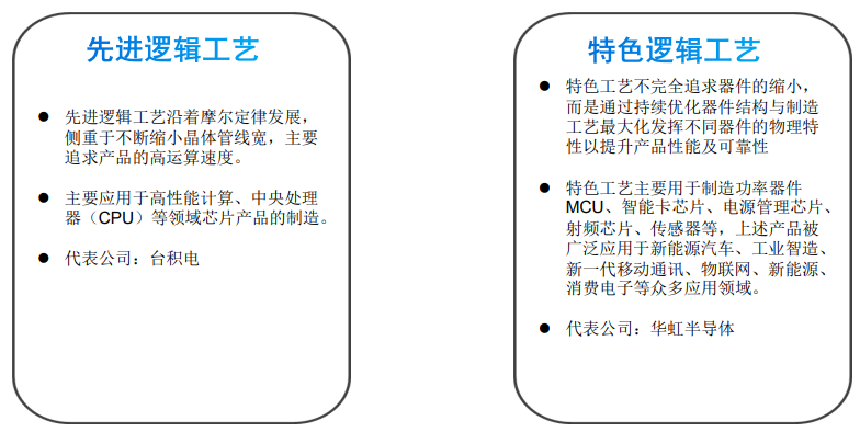
Source: CSDN, Dongxing Securities Research Institute
Taking Hua Hong as an example, Hua Hong is one of the companies with the most comprehensive coverage of specialty process platforms in the industry. The company categorizes its technology platforms based on different products into embedded/standalone non-volatile memory, analog and power management, logic and RF, power devices, etc.
Wafer foundry can be divided into advanced processes and mature processes, with processes below 28nm classified as advanced processes and those at 28nm and above classified as mature processes.
As process nodes evolve, the required investment in equipment has significantly increased
According to IBS data, as process nodes evolve, the required investment in equipment has significantly increased. Specialty processes (generally at 40nm and above) require an investment of two to three billion dollars for every 50,000 wafers of capacity, while advanced processes (28nm and below) require an investment of at least 4 billion dollars or more, with IBS estimating that the investment required for 2nm approaches 28 billion dollars. In the construction costs of wafer fabs, 20%-30% is used for building construction, while 70%-80% is used for equipment investment, and the development of advanced processes has also driven capital expenditures corresponding to unit capacity.
Wafer Foundry 2.0 Concept: Not Limited to Wafer Manufacturing
“Wafer Manufacturing 2.0” includes packaging, testing, photomask production, and others, as well as all integrated device manufacturers (IDM) excluding memory chips. In contrast, the traditional concept of “wafer foundry” is limited to “wafer manufacturing production foundry,” but now, as chip manufacturing becomes increasingly complex, wafer foundries have long since departed from the original simple wafer manufacturing foundry category. The entire production process actually includes packaging, testing, photomask production, and other parts. For example, many AI chips and high-performance computing chips today, TSMC not only provides photomask production and wafer manufacturing services but also offers advanced packaging and testing services. Additionally, some IDM manufacturers have begun to provide wafer foundry services externally. This has effectively broken the original definitions of foundry, outsourced packaging and testing factories, and IDM.
In the first quarter, the wafer foundry 2.0 market revenue reached 72 billion dollars, a 13% increase compared to the same period last year. If we look at the segmented market, traditional wafer foundry market revenue increased by 26% year-on-year; non-memory IDM market revenue declined by 3% year-on-year; the packaging and testing (OSAT) industry performed relatively moderately, with revenue increasing by about 6.8% year-on-year; the photomask market showed good resilience due to the advancement of 2nm processes and the increasing complexity of AI/Chiplet designs, with a year-on-year growth of 3.2%.
For more industry research analysis, please refer to the official website of Sihan Industry Research Institute, which also providesindustry research reports, feasibility reports (project approval, bank loans, investment decisions, group meetings), industry planning, park planning, business plans (equity financing, investment promotion, internal decision-making), special research, architectural design, overseas investment reports and other related consulting service solutions.

 About Us
  Sihan Industry Research Institute Chinasihan.comLeader in Chinese Industry ResearchBuilding a Future City of InnovationContact for Customized Report Orders: · Phone:4008087939 0755-28709360 · Customer Service WeChat:g15361035605 · Customer Service QQ:454058156 · Email:chinasihan@126.com
· Official Website: Chinasihan.com