
Click the blue text to follow us

In the early days of IC design, chip power consumption was not a significant constraint, so it was rarely considered during design. Today, with the demand for longer battery life in mobile phones and IoT devices,chip power consumption has become as important as performance, becoming a key factor in determining product competitiveness.
In this article, we will break down thecore sources of chip power consumption, as well as thelow power design approaches from top to bottom.
The power consumption of a chip mainly comes from three sources:surge power, static power, and dynamic power.

1
Surge Power
Surge current refers to the maximum instantaneous input current generated when a device is powered on. Therefore, in applications, surge current is also referred to as startup current.
Although the surge current lasts for a very short time, generally between nanoseconds to microseconds, the peak current is very high, which can put instantaneous pressure on power supply design and heat dissipation, making it a special scenario to consider in low power design.

2
Static Power
Static power mainly refers to power consumption caused by leakage current. This leakage current mainly includessub-threshold leakage current between the source and drain of transistors, as well astunneling leakage current between the gate and substrate. Therefore, leakage current occurs whether the device is switching or not.
The formula for calculating static power is as follows:

Where, Vdd is the supply voltage, ILeakage is the leakage current.

3
Dynamic Power
Dynamic power includesswitching power and short-circuit power.
(1)Switching Power
When the output signal of a logic gate switches, the power consumed due to charging and discharging the load capacitance is called switching power.
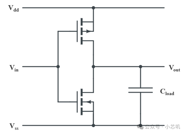
CMOS NOT Gate
For example, in the above CMOS NOT gate,
-
When Vin=0, PMOS is on, NMOS is off, at this time Vdd charges the load capacitance Cload, pulling Vout high.
-
When Vin=1, PMOS is off, NMOS is on, at this time the load capacitance Cload discharges through NMOS, pulling Vout low.
The formula for calculating switching power is as follows:

Where, Cload is the load capacitance, Vdd is the supply voltage, f is the signal switching frequency.
(2)Short-Circuit Power
The signal transition does not occur instantaneously. Therefore, during the input signal transition, NMOS and PMOS are both on for a period of time, creating a path from Vdd to GND, resulting in short-circuit current.
The formula for calculating short-circuit power is as follows:

Where, Vdd is the supply voltage, Q is the charge caused by the short circuit from Vdd to GND during the transition, f is the signal switching frequency.
Therefore, the total power consumption of the chip is defined as:

From the definition of total power consumption, it can be seen thatreducing supply voltage, load capacitance, and signal switching frequency is the core direction for reducing total power consumption.
Low power design is not a separate effort at any one stage, but should be carried out at all design levels, meaning that there should be design techniques to reduce power consumption at the system level, architecture level, logic level, and transistor level.
Although power consumption can be reduced at various design levels,the higher the design level, the more effective the power reduction, and the lower the design stage, the smaller the optimization space for power consumption. Therefore, reducing power consumption at the system level and architecture level can achieve better results.
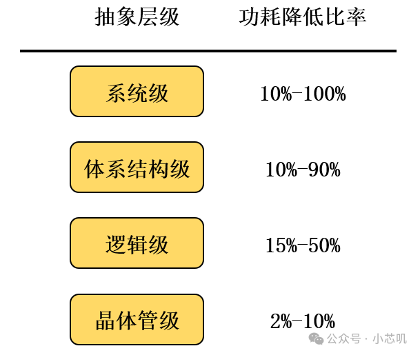
Power reduction ratios at different levels
-
System Level
The system level can directly determine the functional allocation of the chip and the top-level strategy of the power architecture,this stage directly determines the power consumption baseline of the chip, with the greatest potential for power optimization.
-
Architecture Level
The architecture of the chip optimizes the operation mechanism of core modules under the system-level framework, such as choosing to use parallel structures or pipelined structures.
Although the optimization ceiling is limited by the system-level architecture, it can still lead to significant power reduction,making it a key optimization stage for high-performance low-power chips.
-
Logic Level
At the logic level, power optimization is already limited to adjustments within determined modules, unable to change the redundancy of the top-level architecture, resulting in a smaller power optimization ratio.
-
Transistor Level
At the transistor level, it is alreadythe physical layer method for optimizing power consumption, limited by the manufacturing process of the devices, can only slightly reduce power consumption.
Low power design of chips has become a cross-disciplinary system engineering, requiring good planning at the top-level architecture and meticulous refinement in the bottom-level implementation. In subsequent articles, we will introduce commonly used low power design techniques for chips at various levels from system level to transistor level.
Thank you for reading my article. If you find it useful, please give me afollow. Let’s continue the conversation next time.
>/ Author: Xiao Xin Ji