MCUMicro Classroom
CKS32K148 LPI2C
Issue 60 2025.09.16
LPI2C (Low Power Inter-Integrated Circuit) is a low-power I2C interface module in the CKS32K148 microcontroller. The CKS32K148 MCU features two LPI2C modules, LPI2C0 and LPI2C1, supporting communication rates of standard mode (100 kbps), fast mode (400 kbps), fast+ mode (1 Mbps), and high-speed mode (3.4 Mbps).

Main Features
Compatibility: Supports I2C bus standard mode, fast mode, fast+ mode, and high-speed mode (HS) in slave mode.
Low Power: Supports low-power mode.
Multi-Master Mode: Supports multi-master operation, including synchronization and arbitration mechanisms.
Interrupt and DMA Support: Provides interrupt and DMA support to reduce CPU load.
Configurability: Configurable broadcast calls, 7-bit or 10-bit address modes. Clock sources can be selected from SOSC, SIRC, FIRC, and SPLL, with clock stretching and timing configurable via registers.
Error Detection: Supports bus busy detection, arbitration loss, FIFO errors, port low-level timeout, and bit error detection.
Master Features
-
4-depth command/send/receive FIFO
-
Command FIFO waits for idle I2C bus: Before starting transmission, the command FIFO waits for the I2C bus to be idle
-
Command FIFO supports initiating (repeated) START and STOP conditions: Can initiate one or more master receiver transmissions
-
STOP condition can be generated from the command FIFO or automatically generated when the send FIFO is empty
-
Master request input: Used to control the start time of I2C bus transmission
-
Flexible data matching function: Can generate interrupts on data matches and discard unnecessary data
-
Flags and optional interrupts: Indicate repeated START conditions, STOP conditions, arbitration loss, unexpected NACK, and command word errors
-
Supports configurable bus idle timeout and pin low-level timeout: Enhances bus robustness and reliability
Slave Features
-
Independent I2C slave registers: Reduces software overhead caused by master/slave switching
-
Supports 7-bit or 10-bit addresses, address ranges, SMBus alerts, and general call addresses: Provides flexible address configuration and communication capabilities
-
Send/receive data registers support interrupt or DMA requests: Facilitates efficient data transmission and reception
-
Software controllable ACK or NACK: Supports optional clock stretching on ACK/NACK bits
-
Configurable clock stretching: Prevents send FIFO underflow and receive FIFO overflow errors
-
Flags and optional interrupts: Indicate packet end, STOP conditions, or bit error detection

Master/Slave Data Transmission
The LPI2C block diagram of the CKS32K148 series MCU is shown below:
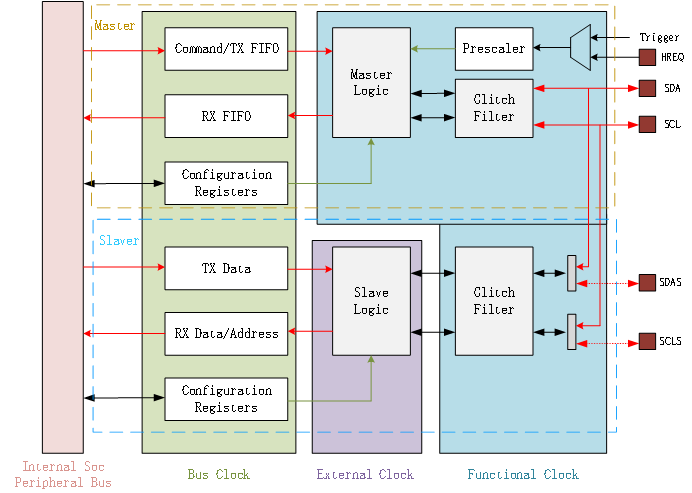
Figure 1 LPI2C Block Diagram
The LPI2C master and slave controller logic operates independently to perform all master/slave mode transmission tasks separately on the I2C bus. This independence allows the master/slave controllers to efficiently manage bus communication, enhancing system flexibility and performance.
LPI2C Ports
LPI2C supports different port configuration modes under various external conditions, configured through the MCFGR1[26:24] register.
Open-drain support: The LPI2C master device defaults to configuring the SDA and SCL pins in open-drain mode.
High-speed mode support: High-speed mode support also depends on the specific device and requires the SCL pin to support the current source pull-up required by the I2C specification.
Ultra-fast mode support: The LPI2C master device also supports push-pull functionality required for I2C ultra-fast mode using SDA and SCL pins. Enabling ultra-fast mode also requires setting the MCFGR1[IGNACK] bit.
Push-pull dual-line support: The LPI2C master device also supports push-pull dual-line configuration, which can support partial high-speed mode if LPI2C is the only master device and all I2C pin voltages on the bus are the same.
Push-pull quad-line support: The push-pull quad-line configuration uses SCL/SDA pins for input data; SCLS/SDAS pins for output data, with configurable polarity. Note that when using this quad-line configuration, the LPI2C master device logic and LPI2C slave device logic cannot connect to a separate I2C bus.
LPI2C Master Transmission
When LPI2C is enabled, it continuously monitors the I2C bus to detect whether the bus is idle (via the MSR[BBF] flag). When a bus idle timeout is detected (configured by MCFGR2[BUSIDLE]) or a STOP condition occurs, the I2C bus is considered idle.
After the I2C bus is idle, if the send FIFO is not empty and the master request is triggered or disabled, the LPI2C master controller will initiate transmission on the I2C bus. This process includes the following steps:
-
Wait for bus idle time
Wait time = (MCCR0[CLKLO] + 1) * prescaler (MCFGR1[PRESCALE]).
-
Send START condition and address byte
Send START condition and address byte using timing configuration in the master clock configuration register 0 (MCCR0); if configured for high-speed mode transmission, use timing configuration in the master clock configuration register 1 (MCCR1).
-
Execute master send or master receive transmission
Execute master send or master receive transmission based on the configuration of the send FIFO.
-
Send NACK in the last master receive transmission
Unless the next command in the send FIFO is also a receive data command and the send FIFO is not empty, send NACK in the last master receive transmission.
-
Send repeated START or STOP condition
Send repeated START or STOP condition based on the configuration of the send FIFO and/or MCFGR1[AUTOSTOP].
When the LPI2C master controller is disabled (either due to MCR[MEN] being cleared or due to the mode entering auto-disable), LPI2C will continue to empty the send FIFO (after the send FIFO is empty, LPI2C will automatically generate a STOP condition) until the STOP condition is sent.
LPI2C Slave Transmission
Before LPI2C is enabled, the slave address can be set for matching: supports 7-bit or 10-bit address modes, and the address can be configured for matching range.
-
Wait for the master START condition: The slave monitors the I2C bus, waiting for the master to send the START condition and slave address.
-
Address matching: If the received address matches the address configured for the slave, the slave sends an ACK response, and then the LPI2C slave will automatically perform slave transmit or slave receive transmission.
-
Send and receive data: The slave sends data through the send data register STDR; receives data sent by the master through the receive data register SRDR.
-
Handle reception completion: If a STOP condition or packet end is detected, the slave can trigger an interrupt or flag to notify software to process the received data.
LPI2C Master Timing Configuration Description
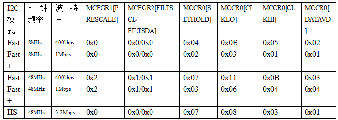
During LPI2C communication, timing parameters must be configured to meet the requirements of the I2C specification; this will depend on the supported modes and the LPI2C functional clock frequency. The following table provides examples of register timing configurations under different modes:
Table 1 Register Timing Configuration

LPI2C Master-Slave Communication Example
1. Configure LPI2C Clock
CLOCK_DRV_Init(&clockMan1_InitConfig0);
Where “clockMan1_InitConfig0” contains clock configurations for SIRC, FIRC, SOSC, PLL, and the LPI2C peripheral (within the peripheralClockConfig0 structure).
peripheral_clock_config_t peripheralClockConfig0[NUM_OF_PERIPHERAL_CLO CKS_0] = {
…
{
.clockName = LPI2C1_CLK,
.clkGate = true,
.clkSrc=CLK_SRC_SIRC_DIV2,//LPI2C clock selection: SOSC/SIRC/FIRC/SPLL
.frac = MULTIPLY_BY_ONE,
.divider = DIVIDE_BY_ONE,
},
…
}
2. Configure LPI2C Pins
PINS_DRV_Init(NUM_OF_CONFIGURED_PINS0, g_pin_mux_InitConfigArr0);
Where “g_pin_mux_InitConfigArr0” contains the configuration for LPI2C pins:
pin_settings_config_t g_pin_mux_InitConfigArr0[NUM_OF_CONFIGURED_PINS0] = {
…
{//LPI2C SDA pin settings
.base = PORTC,
.pinPortIdx = 31U,
.pullConfig = PORT_INTERNAL_PULL_UP_ENABLED,
.driveSelect = PORT_LOW_DRIVE_STRENGTH,
.passiveFilter = false,
.mux = PORT_MUX_ALT4,
.pinLock = false,
.intConfig = PORT_DMA_INT_DISABLED,
.clearIntFlag = false,
.gpioBase = NULL,
.digitalFilter = false,
},
{//LPI2C SCK pin settings
.base = PORTE,
.pinPortIdx = 1U,
.pullConfig = PORT_INTERNAL_PULL_UP_ENABLED,
.driveSelect = PORT_LOW_DRIVE_STRENGTH,
.passiveFilter = false,
.mux = PORT_MUX_ALT4,
.pinLock = false,
.intConfig = PORT_DMA_INT_DISABLED,
.clearIntFlag = false,
.gpioBase = NULL,
.digitalFilter = false,
},
…
}
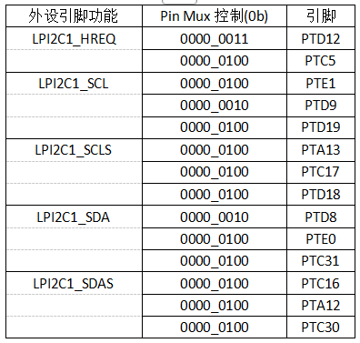
The following table shows the resource allocation of PINs for LPI2C0 and LPI2C1 in the MCU:
Table 2 LPI2C0 Peripheral Pin Multiplexing
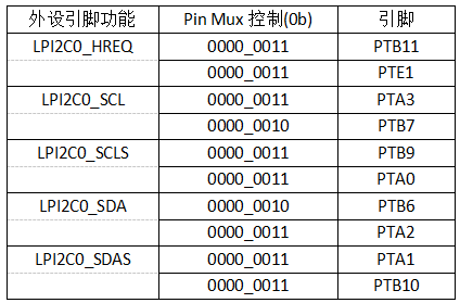
Table 3 LPI2C1 Peripheral Pin Multiplexing
3. LPI2C as Master Sending and Receiving Data
LPI2C as master configured to communicate with slave address 50 at FAST mode 400K rate, with the following parameters:
lpi2c_master_user_config_t lpi2c1_MasterConfig0 = {
.slaveAddress = 50U,//Address configuration
.is10bitAddr = false,//10-bit address configuration
.operatingMode = LPI2C_FAST_MODE,//Mode configuration
.baudRate = 400000UL,//Baud rate setting
.transferType = LPI2C_USING_INTERRUPTS,//Transfer method
.dmaChannel = 0U,//DMA channel if enabled
.masterCallback = NULL,//Interrupt function
.callbackParam = NULL
};
LPI2C_DRV_MasterInit(INST_LPI2C1,&lpi2c1_MasterConfig0,&lpi2c1MasterState);//Initialize LPI2C as master
LPI2C_DRV_MasterSendDataBlocking(INST_LPI2C1, masterTxBuffer, BUFF_SIZE, true, OSIF_WAIT_FOREVER);//LPI2C sends data as master
while(!((LPI2C1->MSR)&LPI2C_MSR_SDF_MASK))//Stop bit detection
{
LPI2C_DRV_MasterReceiveDataBlocking(INST_LPI2C1,masterRxBuffer, BUFF_SIZE, true, OSIF_WAIT_FOREVER);//LPI2C receives data as master
}
1. LPI2C as Slave Sending and Receiving Data
LPI2C as slave, address set to 50, configured for interrupt reception, with the following parameters:
lpi2c_slave_user_config_t lpi2c1_SlaveConfig0 = {
.slaveAddress = 50U,//Slave address
.is10bitAddr = false,//10-bit address configuration
.operatingMode = LPI2C_FAST_MODE,//Mode configuration
.slaveListening = true,//Listening mode
.transferType = LPI2C_USING_INTERRUPTS,//Interrupt transfer
.dmaChannel = 0U,//DMA channel for slave if configured
.slaveCallback = lpi2c1_SlaveCallback0,//Slave interrupt function
.callbackParam = NULL
};
LPI2C_DRV_SlaveInit(INST_LPI2C1, &lpi2c1_SlaveConfig0, &lpi2c1SlaveState);//Initialize slave
Data transmission and reception in interrupt:
void lpi2c1_SlaveCallback0(i2c_slave_event_t slaveEvent,void *userData)
{
uint32_t instance;
instance = (uint32_t)userData;
switch(slaveEvent)
{
case I2C_SLAVE_EVENT_RX_REQ://Slave receives data
LPI2C_DRV_SlaveSetRxBuffer(instance,slaveRxBuffer, BUFF_SIZE);
break;
case I2C_SLAVE_EVENT_TX_REQ://Slave sends data
LPI2C_DRV_SlaveSetTxBuffer(instance, slaveTxBuffer, BUFF_SIZE);
break;
case I2C_SLAVE_EVENT_TX_EMPTY://Transmission complete
case I2C_SLAVE_EVENT_RX_FULL://Reception complete
break;
case I2C_SLAVE_EVENT_STOP:
SendOK = true;
break;
}
}
//Source: Zhongke Xinxin MCU
Thus, the simple master-slave characteristics and transmission mechanisms of the LPI2C module have been described.
Contact Us:
Address: Room 501, Building B, Xintian Industrial Park, Xianggang Second Road, Xixiang Street, Bao’an District, Shenzhen
Phone: 15989378236
Email: [email protected]