Overview of EMC
Purpose of EMC Design:
-
To ensure that the internal circuits of the product do not interfere with each other, achieving the intended functionality;
-
The electromagnetic interference generated by the product is below specific limit values;
-
The product has a certain resistance to external electromagnetic interference.
Principles of EMC Design:
> Suppress interference sources: By reducing the intensity of electromagnetic interference sources within the device, the energy radiated outward is minimized.
> Cut off propagation paths: By reasonable layout and wiring, the propagation paths of electromagnetic interference are reduced.
> Enhance the device’s anti-interference capability: By optimizing the device structure and circuit design, the device’s resistance to external electromagnetic interference is improved.

EMC Rectification Ideas
> When considering issues, decompose the system into three parts: interference sources, coupling paths, and sensitive circuits; improving any one part can solve the electromagnetic compatibility issues of the system;
> Common methods include: considering the electromagnetic compatibility issues of the product and system from aspects such as shielding, grounding, filtering, and loop design;
> Confirm whether the background noise meets standard requirements;
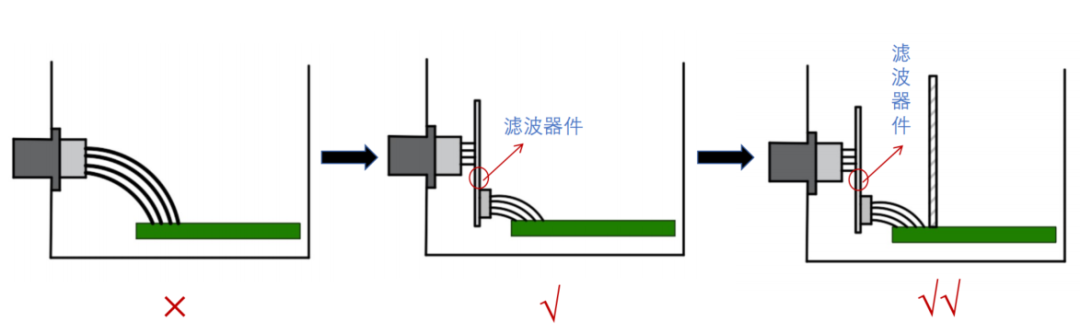
> Check whether the filter is well grounded;
> Ensure that the input and output of the filter are isolated from each other;
EMC Design Approach
> The electromagnetic compatibility of the product is achieved through electromagnetic compatibility design.
> The design of electromagnetic compatibility for products needs to be implemented at different levels, including: component level, part level, PCB level, module level, product level, and integrated system level.
> Solving electromagnetic compatibility issues at the component level, part level, and PCB level is ultimately easier, more effective, and less costly than solving issues at the module level, product level, and integrated system level.
EMC Design Rectification
The PCB is the most fundamental component of electronic products and serves as the carrier for most electronic components. Once the PCB design of a product is completed, it can be said that the disturbance and anti-disturbance characteristics of the core circuit are basically determined. To further improve its electromagnetic compatibility characteristics, one can only rely on filtering of interface circuits and shielding of the enclosure, which not only significantly increases the subsequent costs of the product but also adds to the complexity of the product and reduces its reliability.
PCB EMC design is the foundation of product EMC design. Addressing EMC issues during the PCB design phase is the most effective and cost-efficient means to achieve electromagnetic compatibility for the product.
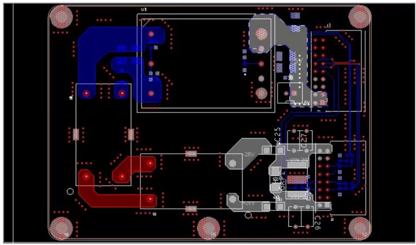
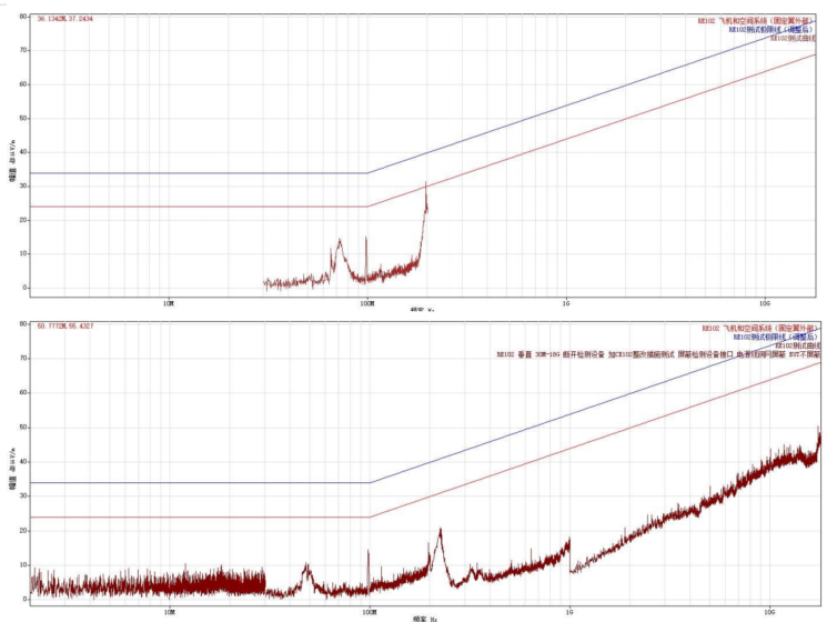
> Before Rectification

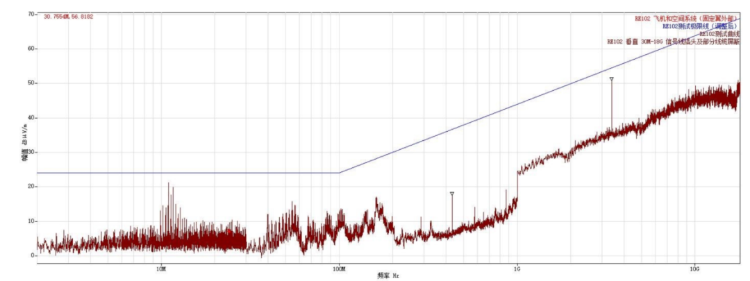
> After Rectification

PCB EMC Design
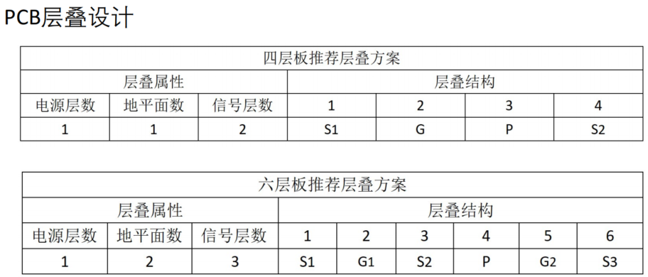

(1) The second or inverted second layer is a complete ground plane G.
(2) The third or inverted third layer is for critical signals (high interference, sensitive), as close as possible to the complete ground plane.
(3) The Vcc layer is adjacent to the complete ground plane.
PCB Layout Design
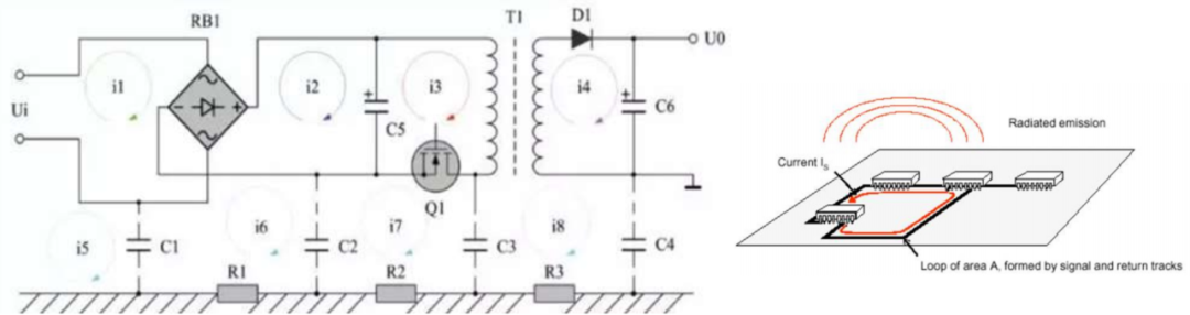
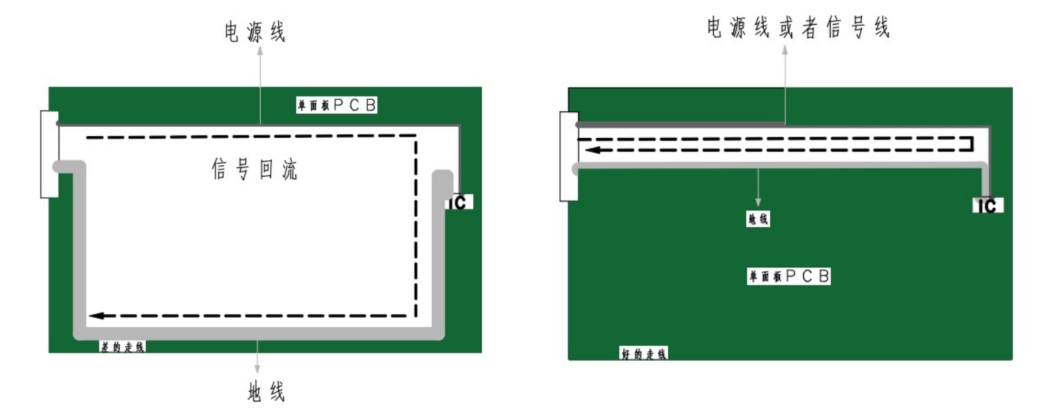
(1) Minimize the effective area of each loop, especially for high-frequency current loops (critical loops), and ensure magnetic shielding for transformers.
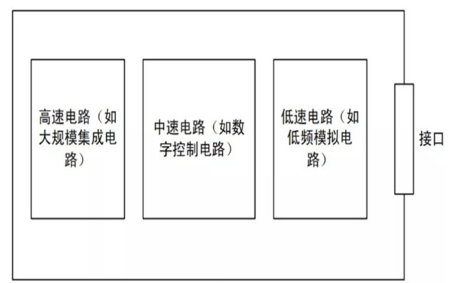
(2) Divide by speed areas.
(3) Divide by functional areas.
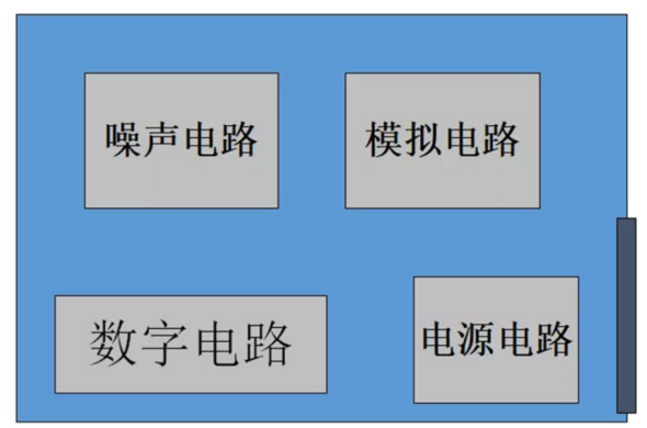
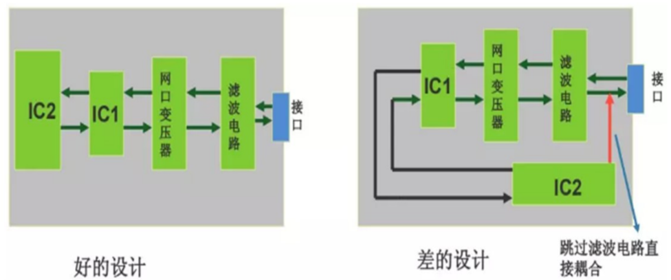
(4) Follow the design principle of placing components in a straight line along the signal flow direction, avoiding back-and-forth routing as much as possible.
PCB Wiring Design
(1) Y capacitors grounding: Common mode inductors should have Y capacitors grounded at both ends, directly connected to the chassis ground as close as possible.
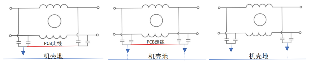
(2) Common mode inductor wiring: Ensure smooth routing for the input and output of common mode inductors, avoiding crossing lines. No other traces should be below the inductor, and all projection layers below should be cut out to prevent interference coupling from the primary and secondary of the common mode inductor.
(3) Capacitor wiring: In PCB wiring, capacitors mainly serve a filtering function. When connecting to GND and power supply, use multiple vias or thicker traces to reduce parasitic inductance.
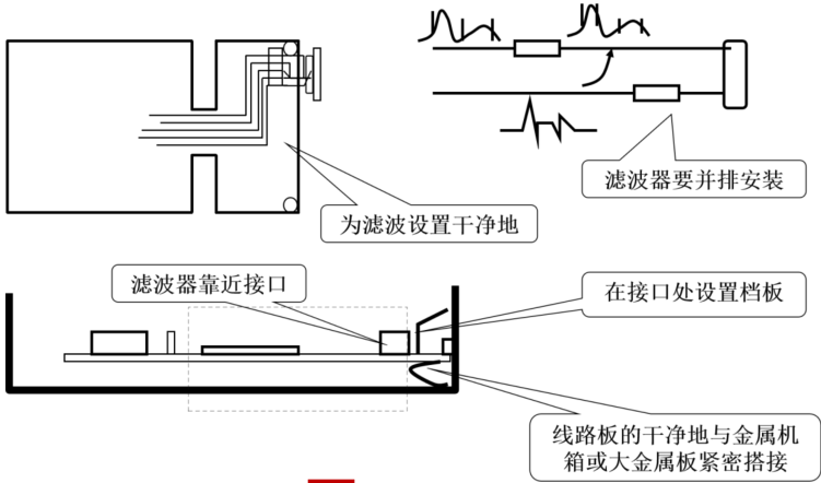
(4) Filter wiring: Ensure that the input and output traces of filters (including filter modules and circuits) are not parallel or crossed, and pay attention to good grounding of the filter.
(5) Wiring should avoid switch chips, crystal oscillators, etc.
(6) Avoid discontinuities in transmission line impedance; points of impedance discontinuity are points of abrupt change in the transmission line, such as sharp corners and vias, which should be minimized.
(7) Power and ground line wiring: Power and ground lines should run parallel to minimize loop area.
(8) Use 45° bends instead of 90° bends in the printed circuit board to reduce high-frequency signal emissions and coupling.
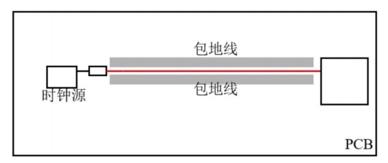
(9) Distribute high-speed lines close to ground plane layers, or run one or two ground lines parallel to high-speed lines to provide shielding and nearby return paths. Fill empty areas with ground. If cost permits, increase the number of ground layers, placing signal layers adjacent to ground plane layers to reduce EMI radiation.
(10) For critical signals (such as clock signals), avoid crossing gaps between split power planes. If crossing is necessary, a coupling capacitor must be placed across the power gap.

PCB Component Layout Design
(1) Considerations for installing filters on the board.
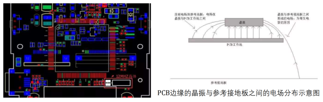
(2) Place the crystal oscillator as close to the processor as possible, and keep the clock line as short as possible. The enclosure should be grounded, and the clock area should be surrounded by ground. Avoid routing under the quartz crystal and under noise-sensitive components.
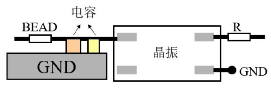
(3) Connect a resistor of about 22 ohms in series with the output of the clock distributor, and ground the unused output pins of the clock distributor through a resistor.
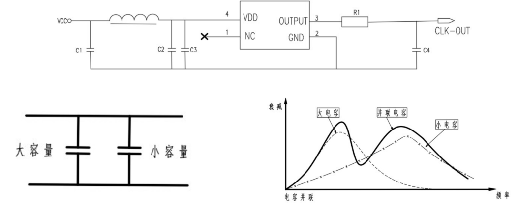
(4) Capacitors must be placed close to the power pins, with a combination of large and small capacitors, and the smaller capacitors should be closer to the power pins.
System Functional Module Structural Layout Design
For systems with multiple functional boards, such as power boards, power amplifier boards, digital control boards, and analog boards, pay special attention to their relative positions.
a. Prevent interference coupling between upper and lower cavities.
b. For modules with strong interference, consider a split cavity shielding design.
c. For sensitive modules, consider a shielding design.
d. Keep sensitive devices as far away from interference sources as possible, properly separate output and input areas, and separate high-level cables and pulse leads from low-level ones.
Internal Cable Layout Design
Product Enclosure Gap Overlap Design
a. It is recommended to use a maze design for the overlap of structural enclosures.
b. For long seams in structural enclosure overlaps, the distance between fastening points or welding points should not exceed 10 cm, minimizing the maximum length dimension.
c. Overlap surfaces should have good conductivity.
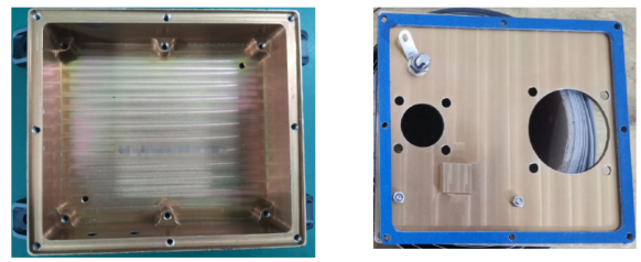
Product Enclosure Opening Design
a. Round holes (typical value Ø3) are preferred for openings, followed by square holes, avoiding long slots. Keep as far away from interference sources as possible.
b. The maximum length dimension of openings should not exceed λ/20 corresponding to the internal interference signals of the enclosure.

EMC Design Rectification
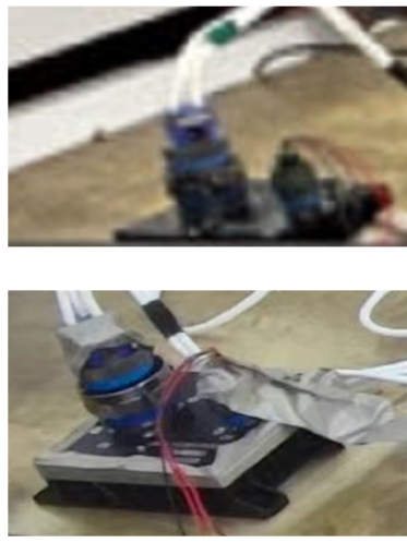
Product Cable Shielding Overlap Treatment
a. The overlap impedance requirement between the connector and the chassis shielding body should meet ≯50mΩ.
b. The connector and the chassis shielding body need to achieve 360° overlap, and additional shielding materials should be added if necessary.
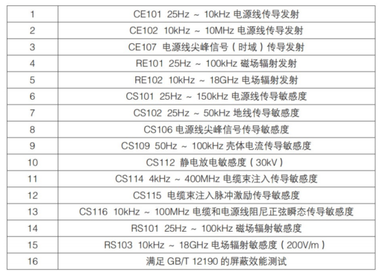
c. According to GJB151B-2013 standards, power lines should use unshielded cables; however, for other cables, shielded cables are recommended.
e. It is recommended that the braid density of external cable shielding should not be less than 90%.
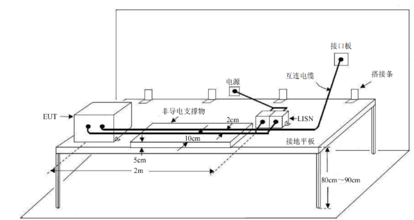
General Testing Configuration