A collection of quick questions and answers about PCB knowledge, your PCB knowledge base!
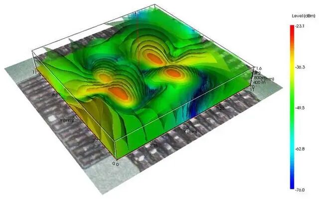

Designing printed circuit boards (PCBs) faces multiple challenges such as size constraints, structural integration, thermal management, and power efficiency. On top of that, electromagnetic compatibility (EMC) issues present additional obstacles for the market launch of new products, further complicating the design process.
Electromagnetic compatibility (EMC) involves a wide range of electromagnetic phenomena, covering the unintended generation, propagation, and reception of electromagnetic energy. EMC issues can not only hinder the normal operation of your circuit board but also interfere with other electronic systems in the vicinity. Different product domains have corresponding EMC standards, but overall, they are quite similar, with corresponding strategies and challenges.
This article aims to explore the most common EMC issues in PCB design and provide practical strategies to reduce the impact of PCB design on board-level EMC.

Board Stack-Up
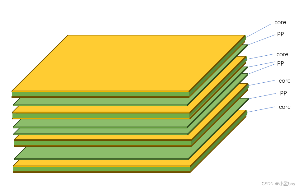
The stack-up of a circuit board defines and arranges the conductive and non-conductive layers within the PCB. The properties of these layers are defined as follows:
-
Conductive layers: Number, order, materials, and copper thickness.
-
Non-conductive layers: Number, order, dielectric materials, and height.
The design range of PCBs can vary from basic single-layer boards to very complex multi-layer systems. Due to the increasing demand for high-frequency signals and miniaturization of components, most modern PCBs adopt a design of 4 layers or more.
Proper arrangement of these layers can bring numerous benefits to the PCB’s EMC (electromagnetic compatibility) and signal integrity performance. This makes stack-up design one of the most critical decisions in new PCB design.
Careful planning of the stack-up structure—including reasonable layer order, grounding, and shielding—can minimize crosstalk and impedance mismatches. Modifying the stack-up structure in the later stages of the PCB design cycle can be very difficult and time-consuming. Therefore, establishing a robust PCB stack-up scheme in the early stages of design can save you a significant amount of time and effort.

Parasitic Impedance
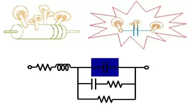
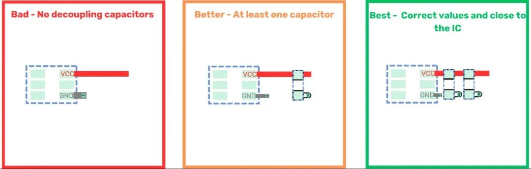
PCB traces inherently possess certain resistance, inductance, and capacitance. This unintended impedance, which is not required by design, is known as parasitic impedance. Minimizing this harmful impedance is crucial for ensuring signal integrity and electromagnetic compatibility (EMC).
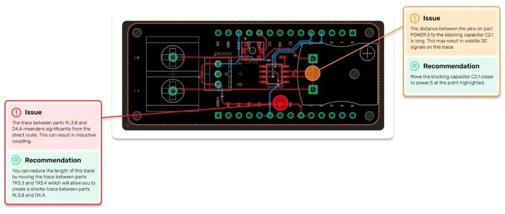
In your PCB design, you can reduce parasitic impedance by using short and wide traces between components. Additionally, proper component layout plays a key role.

Return Paths
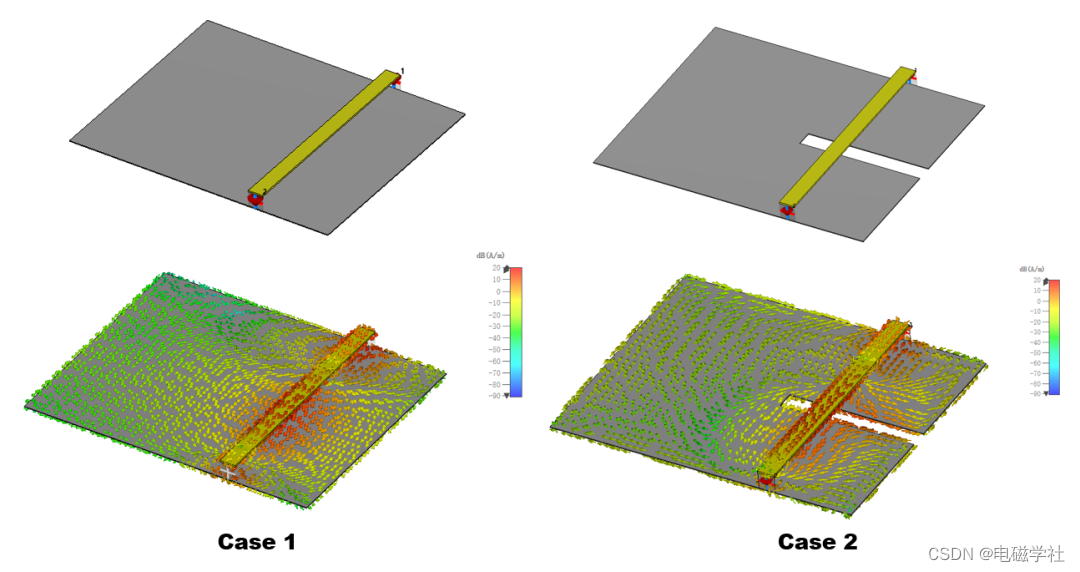
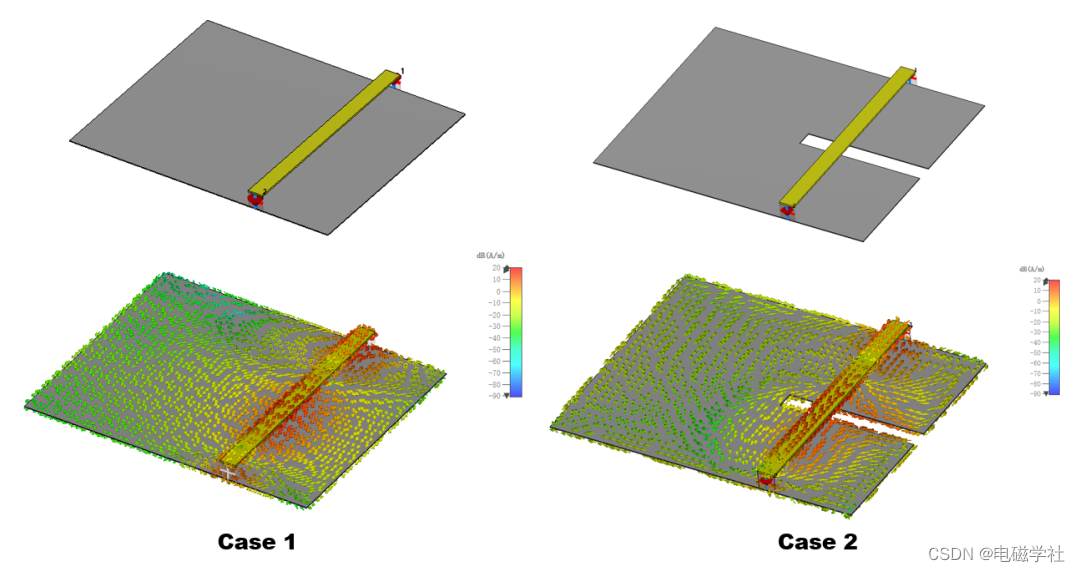
All currents flow out from the source and return to the source, forming a complete circuit loop. The return current will always choose the path of least impedance. At low frequencies, this path is determined by the lowest resistance; while at mid to high frequencies, the return current will flow along the path of least inductance.
To avoid unnecessary electromagnetic radiation and coupling, return paths should be as short as possible. This can be achieved by following these basic guidelines:
-
Keep the distance between components as close as possible, especially for components driving signals with fast rise times.
-
Use large ground planes to minimize inductance.
-
Adopt a stack-up design that can shorten return paths.
-
Avoid splits or gaps in the ground plane.

Ground Connections and Reference Planes
Ground provides a stable reference point for electrical signals. If connected to ground through long traces or poor-quality copper planes, unintended parasitic effects will be introduced.
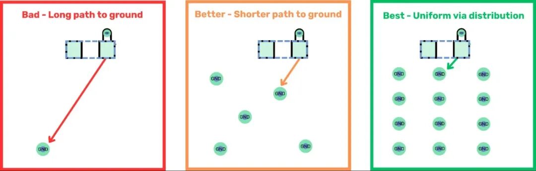
Providing a short return path to ground ensures a low-impedance return path. This also minimizes the possibility of forming ground loops, which can generate radiated emissions and degrade signal integrity and electromagnetic compatibility (EMC).
Reference planes are large areas of copper foil that provide return paths for ground currents and reference points for high-frequency signals. Reference planes are essential for transmission line design and are an efficient and cost-effective solution for controlling electromagnetic radiation.
We often see large areas of copper foil on different layers of PCBs. However, the impedance of these copper areas is not zero, thus introducing inductance, capacitance, and resistance. To minimize the impact of this non-ideal impedance, return paths must be as short as possible in an electrical sense. This also means that when designing connections between ground planes on different PCB layers, their low-impedance characteristics must be ensured.

Stitching Vias
Low impedance between reference planes can be achieved by using stitching vias. By evenly distributing vias along the reference plane, the impedance between them can be significantly reduced, thereby minimizing parasitic effects.
The greatest advantage of this technique is that it does not increase the cost or manufacturing complexity of the PCB.

Crosstalk
Placing long traces too close to each other can negatively impact signal integrity and electromagnetic compatibility (EMC). The electromagnetic field generated by one trace interacts with adjacent traces, leading to unnecessary signal coupling. This phenomenon is known as crosstalk.
To reduce crosstalk:
-
Increase the distance between adjacent traces.
-
Reduce the distance between traces and reference planes.
-
Add ground planes between signal layers to constrain the electromagnetic field (providing shielding).
While the first method is easy to implement, it may increase the size of the circuit board. The second method may significantly impact other aspects of the PCB, such as manufacturing processes or impedance control for high-speed traces.
Other techniques for dealing with crosstalk include: avoiding long parallel runs of traces, placing components away from I/O (input/output) interconnects, and isolating high-noise emission sources to different layers in the stack-up.
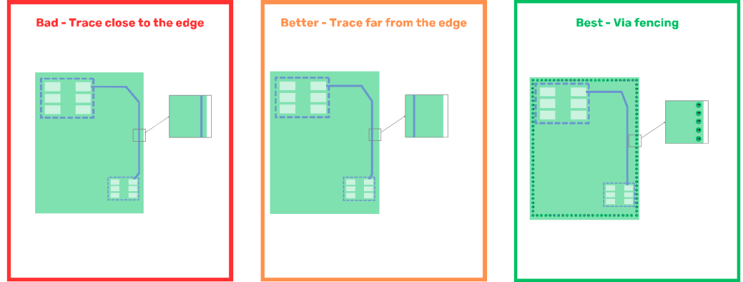

Traces Close to the Board Edges
Traces carrying high-speed digital signals generate strong alternating fields. If these traces are too close to an unshielded edge of the circuit board, these fields may escape the board, resulting in unintended radiated emissions.
Assuming the circuit board has a complete reference plane, follow these guidelines to reduce unintended radiation:
-
Move traces inward from the edge of the circuit board.
-
Add a fence of vias around the entire circuit board for shielding.
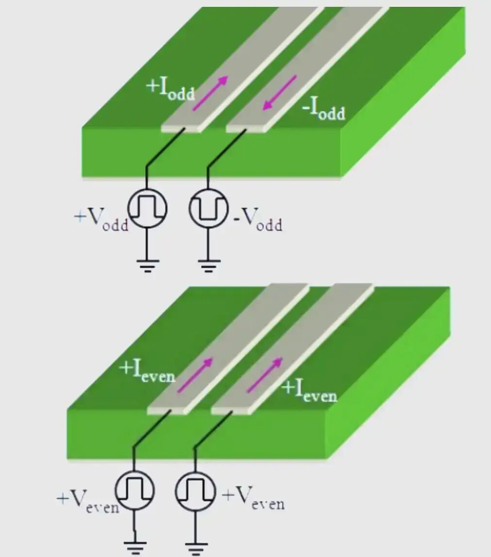

Differential Impedance
Differential pairs are a special type of transmission line where two signal lines are routed in parallel. To avoid signal reflections, differential pairs need to maintain a constant impedance; to avoid signal skew, they need to be of equal length.
To effectively control differential impedance:
-
Control the stack-up of the circuit board by appropriately selecting the thickness and characteristics of the dielectric layers.
-
Place a complete ground plane near the differential pairs.
Only when the reference (ground) plane is located beneath the signal lines is the formula for calculating transmission line impedance valid. If there is no ground plane or if there are gaps in the ground plane, impedance mismatches will occur, leading to signal loss and reflections.

END
Author:CoolDOG007
Source:Smart Chip PlayerCopyright belongs to the original author. If there is any infringement, please contact for deletion..▍Recommended ReadingAn Irresistible VSCode Plugin!A Mobile Operating System Designed Based on FreeRTOSThe Most Legendary American Programmer, Only Using China’s Loongson Computer…→ Follow for more updates ←