
PCB component layout is not a matter of personal preference; it follows certain rules that must be adhered to. In addition to general requirements, some special components have different layout requirements.
Layout Requirements for Crimping Components
1) For crimping components with bent male/female pins, there must not be any components higher than 3mm within 3mm around the component, and no soldered components within 1.5mm; on the reverse side of the crimping component, there must not be any components within 2.5mm of the center of the crimping pin hole.
2) For straight male/female crimping components, there must not be any components within 1mm around the component; if a sleeve is to be installed on the straight male/female crimping component, no components should be placed within 1mm of the sleeve edge; if no sleeve is installed, no components should be placed within 2.5mm of the crimping hole.
3) For European connectors used with grounding connectors, the energized plug-in seat must not have components within 6.5mm of the long pin’s front end and 2.0mm of the short pin.
4) For 2mm FB power single-pin connectors, no components should be placed within 8mm of the front end of the corresponding single-board socket.
Layout Requirements for Temperature-Sensitive Components
1) When laying out components, temperature-sensitive components (such as electrolytic capacitors, crystal oscillators, etc.) should be kept as far away as possible from high-heat components.
2) Temperature-sensitive components should be placed close to the measured element and away from high-temperature areas to avoid interference from other heat-generating components, which could cause erroneous actions.
3) Components that generate heat and are heat-resistant should be placed near air outlets or at the top; however, if they cannot withstand high temperatures, they should be placed near air inlets, ensuring they are positioned away from other heat-generating components and temperature-sensitive components in the direction of rising air.
Layout Requirements for Polarized Components
1) Polarized or directional THD components should be aligned consistently in the same direction and arranged neatly.
2) Polarized SMC components should also be aligned consistently on the board; similar types of components should be arranged neatly for aesthetic purposes.(Polarized components include: electrolytic capacitors, tantalum capacitors, diodes, etc.)
Layout Requirements for Through-Hole Reflow Soldering Components
1) For PCBs with a non-transmission edge size greater than 300mm, heavier components should not be placed in the center of the PCB to reduce the impact of the weight of inserted components on PCB deformation during soldering, as well as the impact of the insertion process on already placed components.
2) For ease of insertion, components are recommended to be placed close to the insertion operation side.
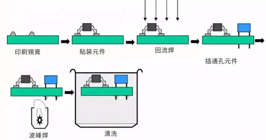
3) For longer components (such as memory module sockets), the length direction is recommended to be aligned with the transmission direction.
4) The distance between the edge of the through-hole reflow soldering component pad and the pitch ≤ 0.65mm of QFP, SOP, connectors, and all BGA should be greater than 20mm. The distance between other SMT components should be >2mm.
5) The distance between the bodies of through-hole reflow soldering components should be >10mm.
6) The distance between the edge of the through-hole reflow soldering component pad and the transmission edge should be ≥10mm; the distance from the non-transmission edge should be ≥5mm.


Screenshots of Some Electronic Books


Screenshots of Some Course PPTs

【Complete Set of Hardware Learning Materials Collection】