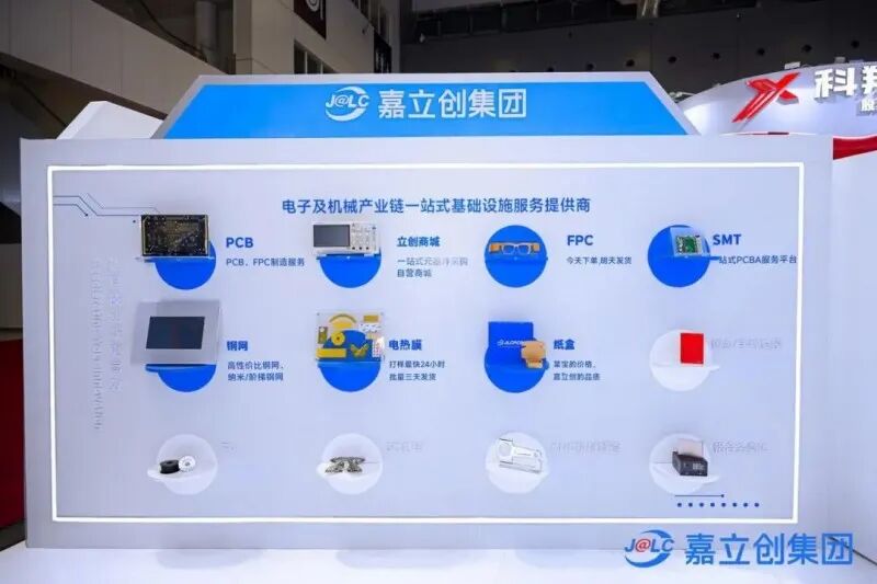
As the global electronics industry evolves towards high performance and miniaturization, printed circuit boards (PCBs), as core foundational components, are becoming crucial for hardware innovation. Jialichuang Group (hereinafter referred to as “Jialichuang”), a one-stop electronic and mechanical industry chain service provider that started with PCB prototyping, recently announced the mass production of 34 to 64-layer ultra-high-density PCBs at the 2025 Electronic Semiconductor Industry Innovation Development Conference, and is set to launch 1 to 3-stage HDI (High-Density Interconnect) boards. This move has attracted market attention, especially in the context of Jialichuang’s planned IPO, where its high-end layout is seen as an important reference for assessing the company’s listing potential.
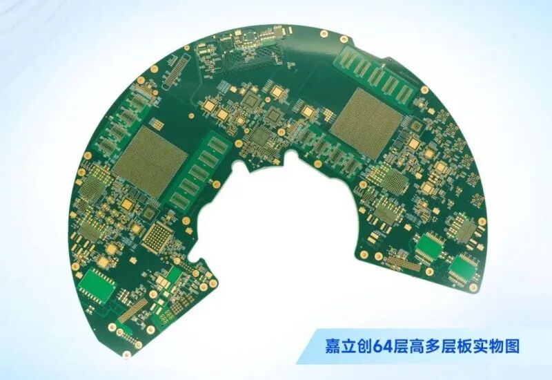
According to data released by Jialichuang, the newly mass-produced 34 to 64-layer ultra-high-density PCBs can achieve a maximum thickness of 5.0mm and a thickness-to-diameter ratio of 20:1, with a minimum line width and spacing of 3.5mil, using Tg170 high-temperature resistant substrates. These parameters meet the demands of high-end industrial control, aerospace, and 5G communication equipment in terms of signal integrity, heat dissipation performance, and structural stability. At the same time, Jialichuang has introduced 0.1mm mechanical micro-drilling technology, enhancing via conduction reliability through industry-leading horizontal copper plating and pulse plating processes. Based on core technologies and supported by an intelligent manufacturing system, Jialichuang has shortened the sample delivery cycle for ultra-high-density PCBs to as fast as 8 days, with prices reduced by about 50% compared to similar products.
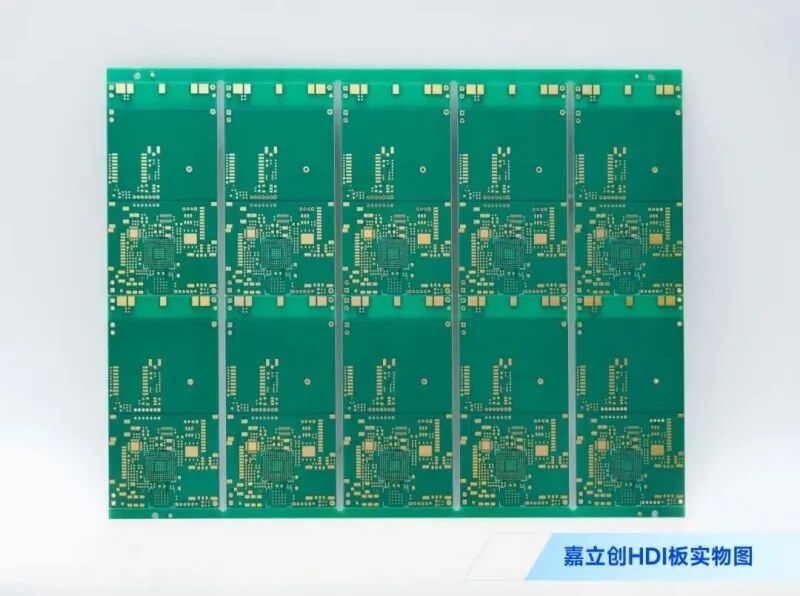
For HDI boards, Jialichuang employs laser drilling technology, controlling the minimum hole diameter to 0.075mm (approximately the thickness of a human hair), and uses Shengyi Technology S1000-2M high-performance materials to meet the needs of smartphones, wearable devices, ADAS radars, and 5G base stations. HDI technology achieves high-density wiring through micro-blind holes and fine line widths, increasing the number of solder points per cm² by 3-5 times, addressing issues of chip pin explosion and signal integrity. Ultra-high-density PCBs support complex functions such as the ultra-thin motherboard of the iPhone or the Tesla FSD computer through vertical stacking of multiple modules.
Jialichuang’s entry into the high-end PCB market is closely related to its long-term technological accumulation. Public information shows that its technology development has gone through several stages: achieving an HDI layer alignment error of ≤5μm in 2018, establishing a demonstration production line for 32-layer boards in 2020, and in 2021, through the integration and upgrading of the entire industry chain, shortening the product development cycle by about 60%, while launching a DFM review system to help developers avoid design risks in advance. In the 2023-2025 intelligent manufacturing phase, the introduction of 5G+AI quality inspection has improved defect detection accuracy to 99.8%.
According to industry data for 2024 cited by Jialichuang’s ultra-high-density PCB and HDI production head, in a PCB market valued at approximately 400 billion yuan, high-end fields such as HDI and ultra-high-density PCBs have high technical barriers, involving core challenges such as inter-layer alignment and signal integrity. Jialichuang’s achievement of mass production for related products marks its technical capability to participate in high-end market competition, officially entering the high-value-added PCB track. An engineer commented after attending Jialichuang’s ultra-high-density PCB and HDI board launch event that Jialichuang has made high-end processes accessible, usable, and reliable for every engineer, providing more confidence for future high-end hardware innovation.