
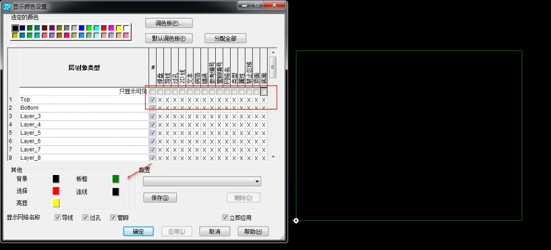
1First, determine the dimensions of the board in the PCB file, as shown in the figure below, with a frame length of 100 mm and a width of 75 mm. 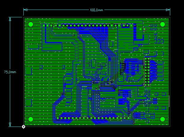 2Open the color display dialog, turn off all unrelated displays, and leave only the board frame.
  3Right-click to select the board frame, then select the entire area of the board frame, press CTRL+C to copy, and CTRL+V to paste. When pasting the board frame, a prompt will appear as shown in the figure below, which can be ignored. Note: Since the PADS software cannot have two board frames, the pasted board frame will automatically change to a 2D line.“
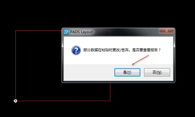 4Place the board frame you want to paste aside for now. Since two board frames cannot exist, it will automatically change to a 2D line after pasting. Click the left mouse button where you want to place it, and you will notice that the line disappears because the 2D line was turned off earlier. In the color display box, check the 2D line to make it visible again.
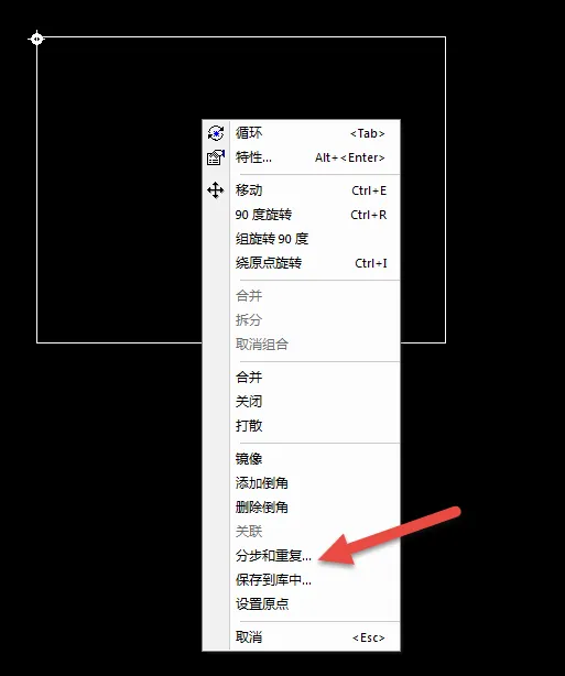 5Select the recently pasted board frame and execute the copy command. Then enter the PCB package editor and paste the copied board frame. Right-click on Distribute and Repeat.
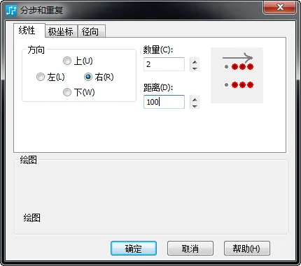 6In the pop-up dialog, select the direction as Right, enter the quantity as 2, and fill in the distance with the previously measured board frame length 100 mm, then confirm.
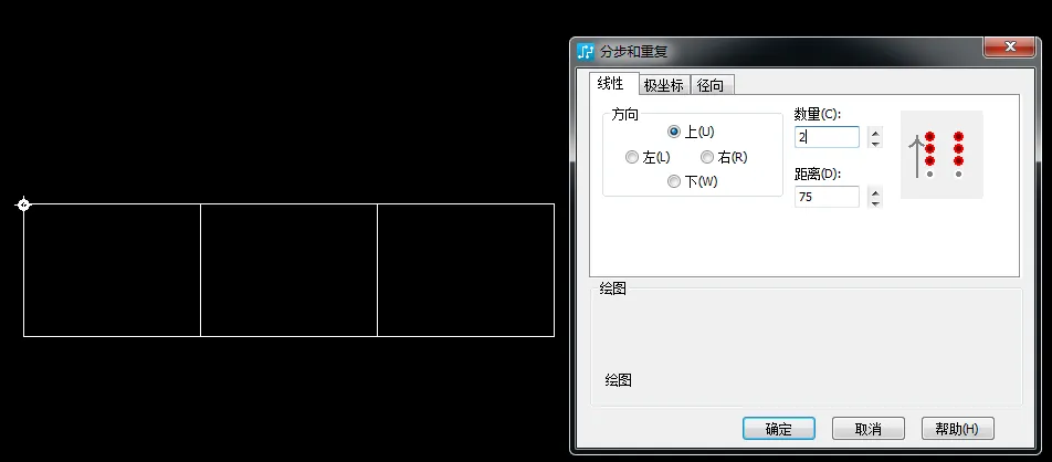 7The result after confirmation is shown in the figure below. Select the three shapes in the image, right-click on distribute and repeat, select the direction as Up, enter the quantity as 2, and fill in the distance with the previously measured board frame width 75 mm, then confirm.
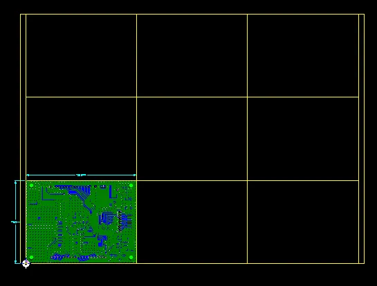
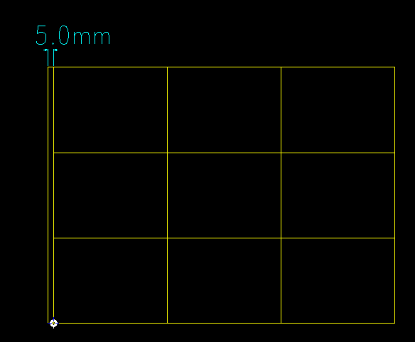 8The effect after distribution is shown in the figure below. You also need to add a 5 mm process margin. Position the origin at the lower left corner of the board frame, change the display grid and design grid to 5 mm, and use a 2D line to draw it. Just draw it on the 5 mm grid, and use the same method to add a 5 mm process margin on the right side.
 9
9
After completing the panelization, select all and copy, return to the PCB interface, and paste it onto the board frame. It is important to note that all board frame diagrams must be placed on ALL layers, and then generate the Gerber files. This concludes the method for panelizing board frames in PADS layout, and I hope it is helpful to everyone.


Screenshots from some electronic books


Screenshots from some course PPTs

【Complete Set of Hardware Learning Materials】