1 Introduction to Xilinx FFT IP
The Xilinx Fast Fourier Transform (FFT IP) core implements the Cooley-Tukey FFT algorithm, which is an efficient method for computing the Discrete Fourier Transform (DFT).
1) Forward and inverse complex FFT, with configurable runtime.
2) Transform size N = 2m, m = 3 – 16
3) Data sampling precision bx = 8 – 34
4) Phase coefficient precision bw = 8 – 34
5) Arithmetic types:
° Unscaled (full precision) fixed-point
° Scaled fixed-point
° Floating-point
6) Fixed or floating-point interface
7) Butterfly rounding or truncation
8) Block RAM or distributed RAM for data and phase factor storage
9) Optional runtime configurable transform point size
10) Runtime configurable expansion schedule for scalable fixed-point core
11) Bit/digit reversal or natural output order
12) Optional cyclic prefix insertion for digital communication systems
13) Four architectures trade off between core size and transform time
14) Bit-accurate C model and MEX functions for system modeling available for download
15) Four operational architectures available
. Pipelined Streaming I/O
. Radix-4 Burst I/O
. Radix-2 Burst I/O
. Radix-2 Lite Burst I/O
2 Introduction to FFT IP Interface
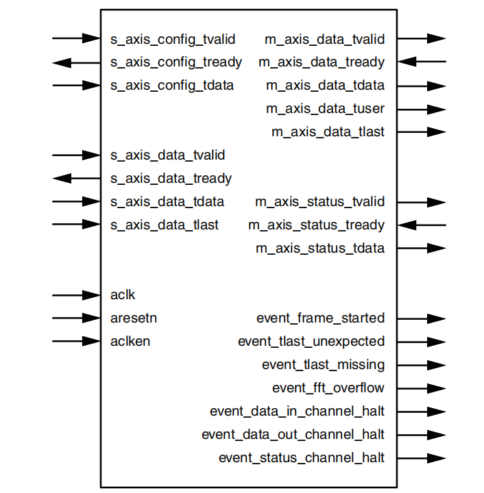
Figure 1 Xilinx FFT IP
1) AXI4-Stream Introduction
The AXI4-Stream interface brings standardization and enhances the interoperability of Xilinx IP LogiCORE solutions. In addition to common control signals such as aclk, acclken, and aresetn, all inputs and outputs to the core are transmitted via the AXI4-Stream channels.Channels are always composed of TVALID and TDATA along with required and optional fields (such as TREADY, TUSER, and TLAST). TVALID and TREADY perform a handshake to transfer messages, where the payload is TDATA, TUSER, and TLAST. The core performs operations on the operands contained in the TDATA field and outputs the results to the TDATA field of the output channel.
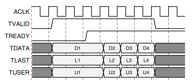
Figure 2 AXI4-Stream Timing Diagram
Figure 2 shows the data transfer in the AXI4-Stream channel. TVALID is driven by the source (master) end of the channel, while TREADY is driven by the receiver (slave). TVALID indicates that the values in the payload fields (TDATA, TUSER, and TLAST) are valid. TREADY indicates that the slave is ready to receive data. A transfer occurs when both TVALID and TREADY are TRUE in a cycle. The master and slave set TVALID and TREADY for the next transfer, respectively.
2) s_axis_config_tdata Interface Introduction
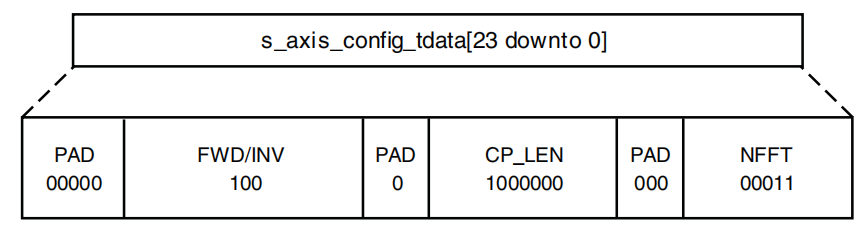
The s_axis_config_tdata interface carries configuration information CP_LEN, FWD / INV, NFFT, and SCALE_SCH.
NFFT (Transform Point Size): NFFT can be the maximum transform size or any smaller point size. For example, a 1024 point FFT can compute point sizes of 1024, 512, 256, etc. The value of NFFT is log2(point size). This field only appears when the transform point size is configurable at runtime.
CP_LEN (Cyclic Prefix Length): The number of samples initially output as a cyclic prefix before outputting the entire transform, starting from the end of the transform. CP_LEN can be any number from zero to less than the point size. This field only appears when cyclic prefix insertion is used.
FWD_INV: Indicates whether to perform a forward FFT transform or an inverse FFT transform (IFFT). When FWD_INV = 1, a forward transform is computed. If FWD_INV = 0, the inverse transform is computed.
SCALE_SCH: Scaling schedule: For burst I/O architecture, the scaling schedule is specified by two bits for each stage, with the scaling of the first stage given by the two LSB. The scaling factor can be specified as 3, 2, 1, or 0, representing the number of bits to shift. For N = 1024, an example scaling schedule for Radix-4 Burst I/O is [1 0 2 3 2] (sorted from last stage to first stage). For N = 128, Radix-2 Burst I/O or Radix-2 Lite Burst I/O, a possible scaling schedule is [1 1 1 1 0 1 2] (sorted from last stage to first stage). For pipelined I/O architecture, the scaling schedule is specified by two bits for every two pairs of Radix-2 stages starting from the two LSB. For example, a scaling schedule for N = 256 could be [2 2 2 3]. When N is not a power of 4, the maximum bit growth for the last stage is one bit. For example, for N = 512, [0 2 2 2 2] or [1 2 2 2 2] are valid scaling schedules, but [2 2 2 2 2] is invalid. For this transform length, the two MSB of SCALE_SCH can only be 00 or 01. This field is only applicable for scaling algorithms (non-scaling, block floating-point, or single-precision floating-point).
The format of the s_axis_config_tdata interface:
1. (Optional) NFFT with padding
2. (Optional) CP_LEN with padding
3. Forward/Inverse
4. (Optional) SCALE_SCH
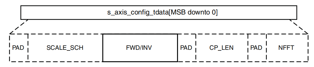
Example:
The core has a configurable transform size, with a maximum size of 128 points, with cyclic prefix insertion and 3 FFT channels. The core needs to be configured to perform an 8 point transform, executing the inverse transform on channels 0 and 1 and the forward transform on channel 2. A 4 point cyclic prefix is required. These fields take the values in the table.
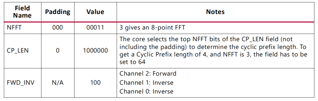
This gives a vector length of 19 bits. Since all AXI channels must be aligned with byte boundaries, 5 padding bits are required, making the length of s_axis_config_tdata 24 bits.
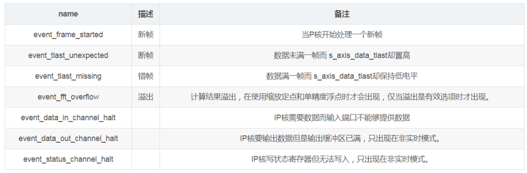
3) Related Flag Signals
3 Simulation Testing of Xilinx FFT IP
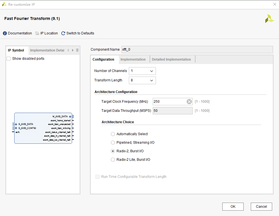
The length of the FFT is selected as 8 points, with the input sequence x = [1,2,3,4,5,6,7,8];
Matlab Verification:
clear allclose allclc x = [1,2,3,4,5,6,7,8];y =fft(x,8);realy=real(y);imagy=imag(y);

The real part output of Y is realy = [36,-4,-4,-4,-4,-4,-4,-4];
The imaginary part output of Y is imagy = [0,9.6569,4,1.6569,0,-1.6569,-4,-9.6569];
FPGA Simulation Verification:
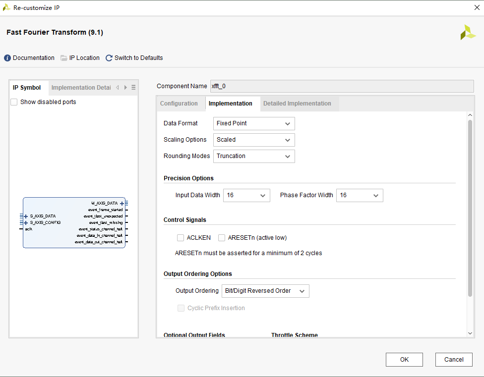
1) IP Settings
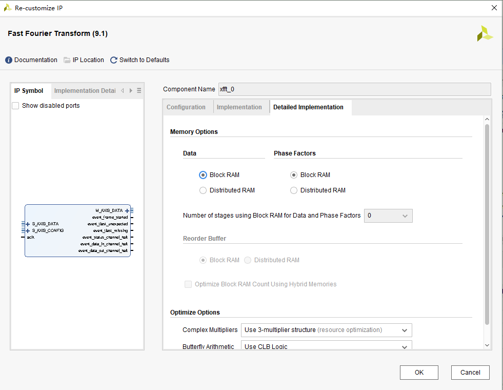
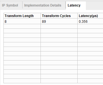
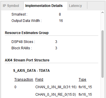
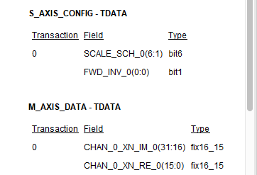
2) Simulation Top Level
`timescale 1ns / 1ps
 module tb_fft_top(     );    reg aclk;                            reg [7 : 0] s_axis_config_tdata;    reg         s_axis_config_tvalid;            wire        s_axis_config_tready;           wire [31 : 0] s_axis_data_tdata;      reg         s_axis_data_tvalid;              wire        s_axis_data_tready;             reg         s_axis_data_tlast;               wire [31 : 0] m_axis_data_tdata;    wire        m_axis_data_tvalid;             reg         m_axis_data_tready;      wire        m_axis_data_tlast;    reg [15:0] real_data;    reg [15:0] imag_data;    wire [15:0] real_dataout;    wire [15:0] imag_dataout;    reg [9:0]  cnt;    assign s_axis_data_tdata={real_data,imag_data};    assign real_dataout = m_axis_data_tdata[31:16];    assign imag_dataout = m_axis_data_tdata[15:0];    initial begin      aclk = 0;      s_axis_config_tdata=8'b0;      s_axis_config_tvalid=1'b0;      s_axis_data_tvalid=1'b0;      s_axis_data_tlast=1'b0;      real_data=16'd0;      imag_data=16'd0;      cnt = 0;      m_axis_data_tready=1'b1;      #1000;      s_axis_config_tdata=8'b0000_0001;      s_axis_config_tvalid=1'b1;      #10;      s_axis_config_tdata=8'b0000_0000;      s_axis_config_tvalid=1'b0;      #1000;      repeat(8)begin        s_axis_data_tvalid=1'b1;        real_data=real_data+16'd1;        cnt=cnt+1;        if(cnt==8) s_axis_data_tlast=1'b1;        #10;      end      s_axis_data_tvalid=1'b0;      s_axis_data_tlast=1'b0;      real_data=16'd0;      #1000;      $stop;    end    always #(5) aclk= ~aclk;fft_top Ufft_top(      .aclk(aclk),                                                // input wire aclk      .s_axis_config_tdata(s_axis_config_tdata),                  // input wire [7 : 0] s_axis_config_tdata      .s_axis_config_tvalid(s_axis_config_tvalid),                // input wire s_axis_config_tvalid      .s_axis_config_tready(s_axis_config_tready),                // output wire s_axis_config_tready      .s_axis_data_tdata(s_axis_data_tdata),                      // input wire [31 : 0] s_axis_data_tdata      .s_axis_data_tvalid(s_axis_data_tvalid),                    // input wire s_axis_data_tvalid      .s_axis_data_tready(s_axis_data_tready),                    // output wire s_axis_data_tready      .s_axis_data_tlast(s_axis_data_tlast),                      // input wire s_axis_data_tlast      .m_axis_data_tdata(m_axis_data_tdata),                      // output wire [31 : 0] m_axis_data_tdata      .m_axis_data_tvalid(m_axis_data_tvalid),                    // output wire m_axis_data_tvalid      .m_axis_data_tready(m_axis_data_tready),                    // input wire m_axis_data_tready      .m_axis_data_tlast(m_axis_data_tlast)                      // output wire m_axis_data_tlast                 );endmodule
3) Simulation Results
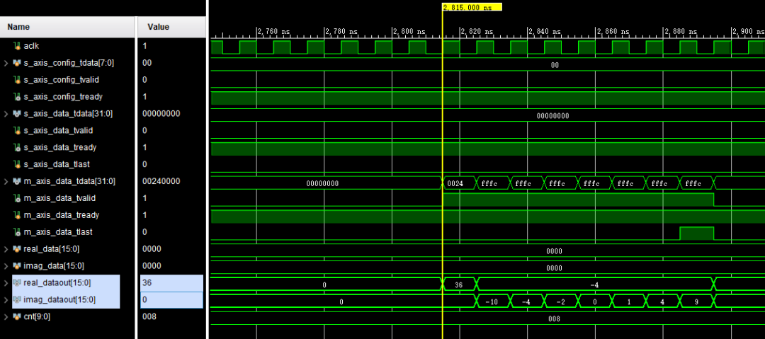
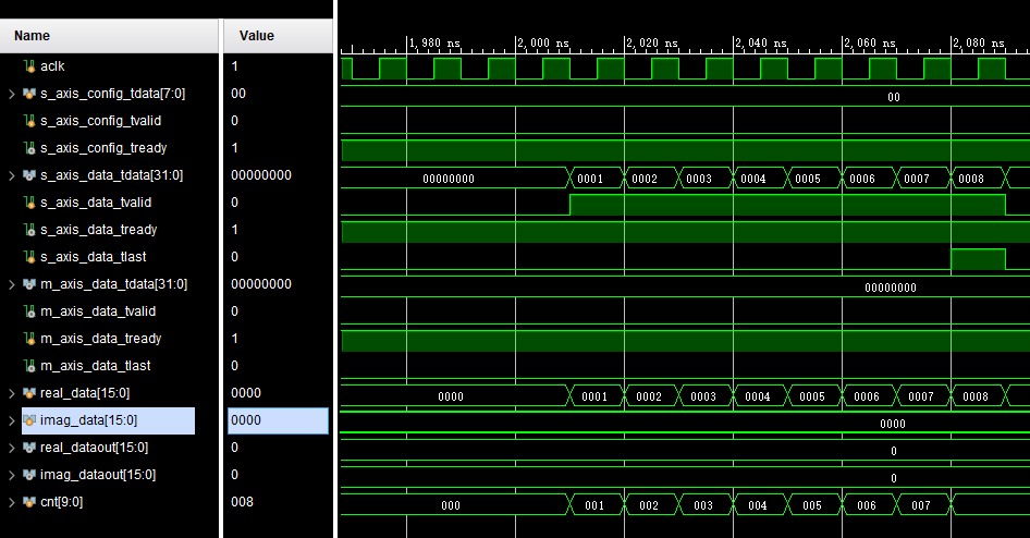
Vivado final simulation results are
Real=[36,-4,-4,-4,-4,-4,-4,-4];
Imag=[0,-10,-4,-2,0,1,4,9];
Compared to the calculations from Matlab, the real part is the same, except for the imaginary part due to data bit truncation issues, where the order of positive and negative parts is reversed.