Having worked in R&D for six years in university laboratories, I first entered the corporate world in 2000 and learned what an “embedded system” truly is. I observed a team of five or six top software experts spend nearly a month optimizing a program that originally fit into 512KB of ROM for a VCD player, ultimately squeezing it down to 256KB. This optimization allowed their clients to reduce the cost of each VCD machine by a few dimes.One of the team members explained to me what embedded systems are: they are systems with severely limited resources; and what makes an embedded expert is someone who can extract maximum performance from a very weak system to achieve seemingly impossible functionalities.Over the years, I have encountered many engineers, especially software engineers who claim to be “proficient in embedded systems” on their resumes. However, after a few questions, I found that they were merely tool-using coders.In my definition, an excellent engineer should be able to achieve set goals under extremely rudimentary R&D conditions, facing severely limited resources, and on a new platform with bugs that no one around has used before.This is also the starting point for all the challenging activities initiated by our company, Yinghe Technology.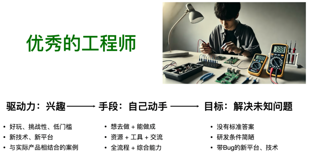 Our user profile at Yinghe TechnologyFor many years, I have wanted to design an MCU version of our “Little Foot” FPGA core board – the Little Foot MCU, so that learners can compare the fundamental differences in programming logic and application scenarios between MCUs and FPGAs. However, I had not found a suitable MCU until the RP2350B with PIO functionality appeared.
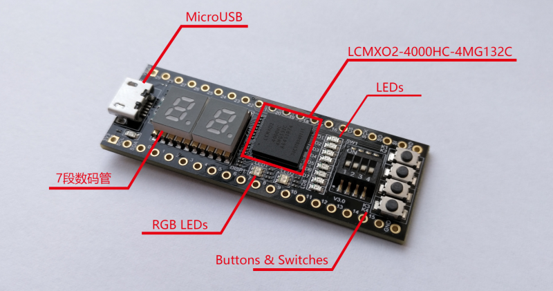 Peripherals on the Little Foot FPGA core board (early version)When I saw the RP2350B, I thought I must use it to realize my vision of the Little Foot MCU. However, I counted the pins and found that the RP2350B has a bit too few; it only has 48 pins. To achieve the same functionality as the Little Foot FPGA core board while retaining 36 IOs for connecting peripheral expansion boards, I needed to use the remaining 12 pins to support:
- 4 tactile buttons,4 switches
- 8 monochrome LEDs
- 2 RGB tricolor lights
- 2 seven-segment displays
- an I2C interface for a posture sensor (which is not even on the Little Foot FPGA, but I want to support it on the MCU board)
This is almost an impossible task! Unless we take an unconventional route! Fortunately, in my youth, I was honored as a “senior hardware engineer” in the company and have experienced countless open-source projects, so handling such IO issues is not too difficult:
- 4 tactile buttons and 4 switches would normally require 8 digital IOs. Can we use an analog method to convert 8 states into 8 different voltage values for the MCU’s ADC to determine? Thanks to the RP2350B’s internal 12-bit ADC, I can save 7 pins! In the final design, I used a common R-2R ladder network used in high-speed DACs to represent these 8 state changes, mainly to introduce a certain level of difficulty for everyone, solving external “imperfect” conditions through software (filtering, debouncing). Embedded systems are not just about software programming; more importantly, it is about “hardware/software collaboration to solve system problems.”
- Can we drive the 8 monochrome LEDs with fewer pins? There is a method called Charlieplexing, which can effectively utilize the three states of IO – high, low, and high impedance, allowing us to drive (4-1) * 4 = 12 LEDs using 4 IOs. Since we only have 8 LEDs on the Little Foot FPGA, we still used 4 IOs to drive 8 LEDs.
- For the 2 tricolor LEDs, we used 6 independent IOs to drive the data lines connected to the LED pins on the Little Foot FPGA. Friends who have played with WS2812B know that you only need one IO to string several WS2812Bs together, so we can save 5 more lines.
- The seven-segment display is the most commonly used display device on the FPGA board. The two displays on our Little Foot FPGA board used 18 IOs to drive them because the FPGA chip with 132 pins has abundant IOs. However, if we used the same method on the RP2350B board, it would consume all 12 remaining IOs, so we had to use a serial-to-parallel conversion method – using two 74HC595s to easily solve this.
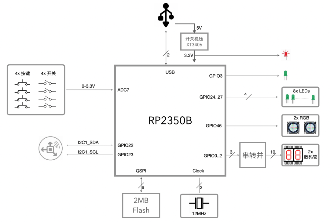 IO configuration on the RP2350B core boardUsing only 9 IOs, I solved the connections for 4 buttons, 4 switches, 8 LEDs, 2 tricolor lights, and 2 displays, leaving 3 IOs spare. I allocated two of the spare IOs for the I2C signal lines for the posture sensor, and the last remaining pin is reserved for the “Hello World” LED that we embedded engineers must use.Some may ask, aren’t there already 8 LEDs on the board? Why do we need another one? This LED is placed at the entrance of programming, and the first operation for beginners is to light it up! Because the 8 LEDs driven by 4 IOs require a certain level of skill to light up after getting started.Thus, all 12 IOs are utilized, neither more nor less, perfectly supporting all peripherals on the Little Foot FPGA board, and fulfilling my long-held wish to add a sensor to the board.This design naturally raises the bar for our users, but these barriers are precisely what learners of “embedded systems” need to master. On our Little Foot MCU board, the IOs are no longer just dumb rods with 0 and 1 states; they are mechanisms, flexible “messengers” that, with the infusion of software’s soul, can interact better with peripherals.For detailed information about this board, please visit:https://www.eetree.cn/platform/4125or click on the “Read Original” link at the end of the article or scan the QR code below to go directly:
 See you next time!Related Reading:
- What Makes a Good MCU Learning Board?
- RP2350B Core Board: Compatible with Little Foot FPGA, Creative Projects Awaiting Unlock!