Abstract: With the rapid development of electronic technology, the types of memory are becoming increasingly diverse, and each type of memory has its unique operation timing. To improve the testing efficiency of memory chips, a multifunctional memory chip testing system has emerged. This paper proposes a hardware design and implementation for a multifunctional memory chip testing system, detailing the interface circuit design for various memory chips with different data widths (SRAM, MRAM, NOR FLASH, NAND FLASH, EEPROM, etc.) and ultimately solves the same-platform testing solution for various memory chips with different data widths, while also detailing the hardware implementation methods for each interface.
Keywords: ABUS; CLAS; NIOSII;
Introduction
With the rapid development of electronic technology, the variety of memory chips is increasing, and their operational methods are completely different. Therefore, a dedicated memory chip tester is required to test a specific type of memory chip. The multifunctional memory chip testing system designed in this paper can perform functional testing on various memory chips such as SRAM, NAND FLASH, NOR FLASH, MRAM, and EEPROM, and each type can be compatible with data buses of 8 bits, 16 bits, 32 bits, 40 bits, etc. If a separate testing platform is designed for each product, the complexity of the testing operations can be imagined. To simplify the testing steps, reduce the complexity of testing, improve testing efficiency, and lower testing costs, a multifunctional memory chip testing system is specifically designed to facilitate and expedite the testing of all the aforementioned memory chips on the same platform.
Design Principle
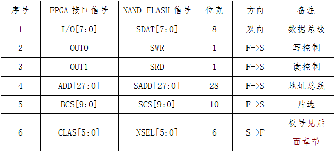
This design scheme adjusts the external bus timing of NIOSII appropriately based on the unique read/write timing access characteristics of the various memories mentioned above, utilizing the flexible programming characteristics of FPGA to ultimately achieve precise operations for reading and writing various memories based on the external bus of NIOSII. As shown in Figure 2-1. An ABUS bus interface is custom-defined through FPGA that can mount all memory chips, as shown in Table 1. Furthermore, the interface can automatically recognize various tested memory chips connected to it, distinguishing them through category input signals (CLAS), where each memory chip corresponds to a unique operational timing. Below are the connection modes and signal descriptions for several types of memory chips. Other memory chips can be connected to the ABUS bus in a similar manner to complete the testing.
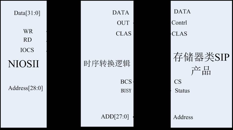
Figure 21: Connection Diagram of Various Memory Chips Mounted on NIOSII Bus
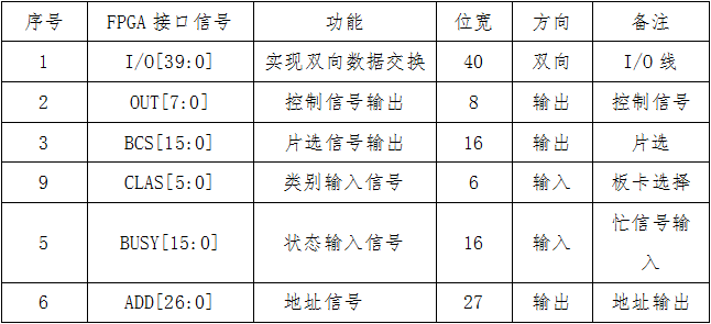
Table 1: ABUS Interface Signal Description Table
40-bit NAND FLASH Connection Design
As shown in Figure 2-2, the 40-bit NAND FLASH is bridged with NIOSII through ABUS (FPGA), completely converting the external bus timing into the operational timing of NAND FLASH. The 40-bit NAND FLASH chip is composed of five independent 8-bit NAND FLASH chips. The external IO ports of the five 8-bit devices are combined into a 40-bit external IO port, while their respective control lines (NCLE, NALE, NRE, NWE) are connected together to form a group of control lines (NCLE, NALE, NRE, NWE), with chip selects independently routed to NCS0-NCS9, and busy signals independently routed to R/B0-R/B9.
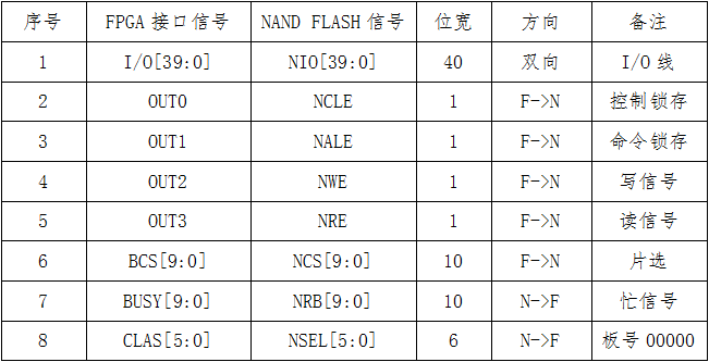
Table 2 details the connection relationship between the 40-bit NAND FLASH and ABUS.
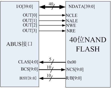
Figure 22: Interface Diagram of ABUS and 40-bit NAND FLASH
Table 2: 40-bit NAND FLASH Interface Connection Table
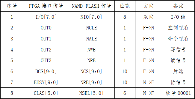
8-bit NAND FLASH Connection with NIOSII
The 8-bit NAND FLASH is constructed by stacking multiple 8-bit NAND FLASH chips, with the external bus and control lines (NALE, CLE, NEW, NRE) of each chip interconnected. Each chip’s chip select and busy signals NCS0-NCS9, NRB0-NRB9 are routed separately. FPGA logic can be used to modify the read/write timing of the NIOSII bus to accurately operate the large-capacity 8-bit NAND FLASH memory module, realizing the connection from NIOSII to ABUS, and from ABUS to the 8-bit NAND FLASH, as shown in Figure 2-3.
Table 3 details the connection relationship between the 8-bit NAND FLASH and ABUS.
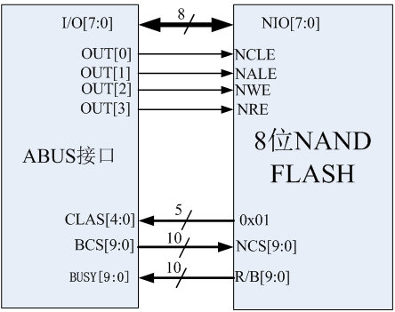
Figure 23: Connection of ABUS and 8-bit Large Capacity NAND FLASH
Table 3: 8-bit NAND FLASH Interface Connection Table
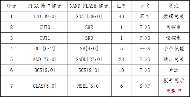
40-bit SRAM Connection with NIOSII
The 40-bit SRAM module is connected to NIOSII through ABUS to achieve correct timing read/write operations. During testing, only 8 bits are tested at a time, completing all space testing in 5 passes as shown in Figure 2-4. Table 4 provides detailed signal connection descriptions.
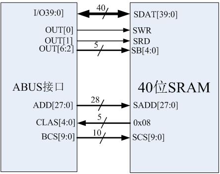
Figure 24: Connection of ABUS and 40-bit SRAM
Table 4: 40-bit SRAM Interface Connection Table
8-bit SRAM Connection with NIOSII
The 8-bit SRAM module is connected to NIOSII via ABUS (FPGA) to achieve correct timing read/write operations as shown in Figure 2-5. Table 5 provides signal connection descriptions.
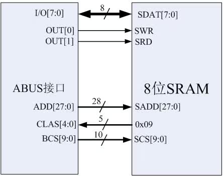
Figure 25: Connection of ABUS and 8-bit SRAM
Table 5: 8-bit SRAM Interface Connection Table
Hardware Circuit Design
Testing the NAND FLASH can take up to ten hours. To improve testing efficiency and speed, this design employs two identical and independent hardware systems. It can test up to 2 NAND FLASH devices simultaneously. Each hardware system consists of a microprocessor (NIOSII), a large-capacity FPGA, and a memory testing expansion interface (i.e., ABUS interface), as shown in Figure 3-1. The RS232 communication interface enables data exchange between the testing system and the host computer, completing human-computer interaction. The power supply system generates various suitable voltages to meet the power supply requirements of each chip.
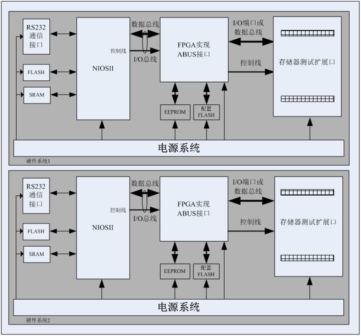
Figure 31: Hardware Block Diagram
Processor Module Circuit
The processor module circuit consists of the embedded NIOSII soft core (CPU) in FPGA, two RS232 communication lines, one FLASH chip, and one SRAM chip. The CPU is the core manager of the entire system, responsible for read/write testing of various memory chips below it and communication with the host computer above it, achieving human-computer interaction. Communication is accomplished by one of the RS232 circuits, while the other RS232 circuit is used for system debugging and software solidification. The FLASH chip is used to store program code and important data, while the SRAM chip, after powering on the CPU, loads the FLASH program through the CPU, ultimately providing a fast operating environment for the CPU’s program code.
FPGA-Based ABUS Interface Module
The ABUS interface module consists of an FPGA chip, configuration FLASH, and data storage EEPROM chip. ABUS interfaces the external bus of NIOSII with various memory modules, with each specific memory having a specific timing logic. Each timing logic can be implemented through FPGA hardware code (IP core). Each memory module will provide a fixed category signal CLAS to the ABUS interface during testing, which will recognize various SIP memory modules based on this category signal, ultimately switching to the correct corresponding specific product timing logic to complete the read/write testing of memory chips via the external bus of NIOSII. The configuration FLASH performs the loading of the hardware program at power-up and protects data during power loss. The EEPROM is used to store important system parameters.
SIP Memory Testing Expansion Interface
The memory testing expansion interface is constructed with two rows of dual-row seats, totaling 120 pins. The ABUS interface connects with the testing expansion interface: 40 pins connect to bidirectional data or I/O lines, 8 pins connect to 8 signal input control lines, 16 pins connect to 16 chip select signal output lines, 5 pins connect to 5 category input signal lines, 16 pins connect to 16 status input signal lines, and 27 pins connect to 27 address lines. The remaining pins can be allocated for power and ground, as well as signal indication, etc.
Design of ABUS Interface IP Core
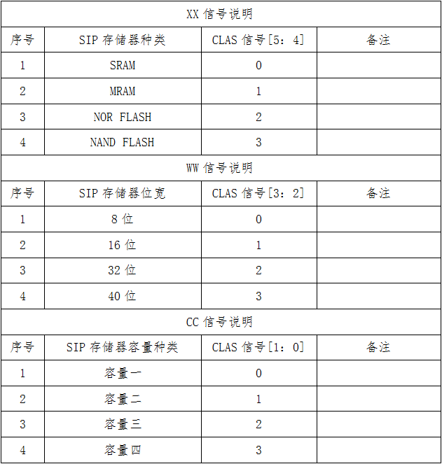
Each SIP memory corresponds to a specific ABUS interface IP core to achieve correct timing read/write operations. This IP core has a unified interface convention, consisting of two fixed interfaces, one of which connects with NIOSII as the external bus interface, operating according to the timing specifications of NIOSII’s external bus, and the other interface is the aforementioned ABUS interface, which, under valid CLAS signals, is responsible for converting the external bus read/write timing of NIOSII into the timing of the corresponding memory chip. The function of the IP core is to complete these read/write operation conversions. Table 5 shows the input values of various SIP memories corresponding to the category signal (CLAS), which must be set according to these values when designing the interface adapter board for the ABUS to switch to the correct read/write timing.
The seven-bit category identification signal has the meaning: T_XX_WW_CC, where T=1 indicates a high-low test, and T=0 indicates a functional test at room temperature. XX represents the type of memory, WW represents the bus width, and CC represents the capacity type.
Table 5: CLAS Signal Values Corresponding to Various SIP Memories
Design of 8-bit SRAM/MRAM/NOR FLASH Interface IP Core
As shown in Figure 4-1, the interface operations of SRAM, MRAM, and NOR FLASH are basically consistent, fully satisfying the bus timing of NIOSII. Therefore, in the FPGA, it is sufficient to simply connect the corresponding control and data lines. Only one chip select register needs to be designed to distinguish the 16 chip selects of the memory chips. Each chip select can access a space of 128MByte. The address of the chip select register is (base address + 0x0FFFFFFC), with the base address set at the highest address of NIOSII’s external bus.
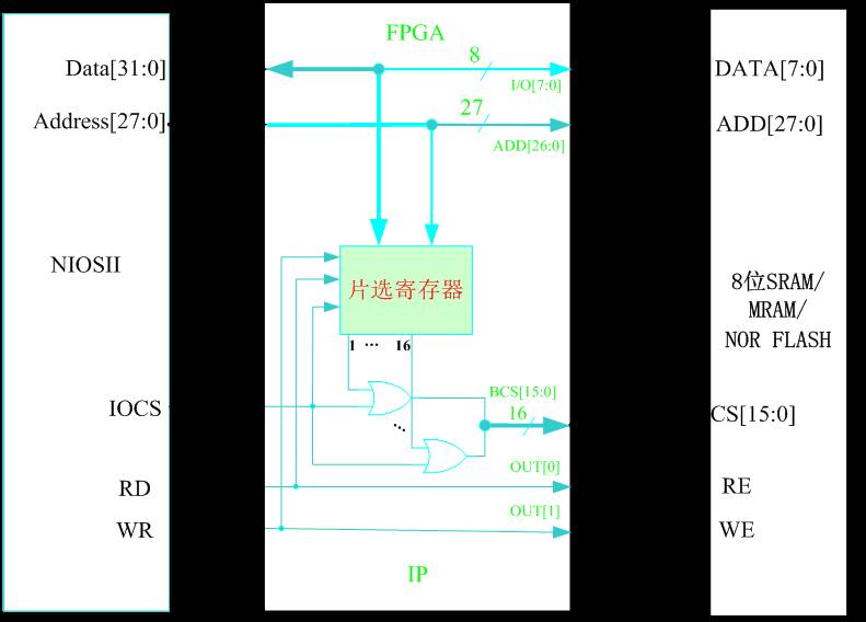
Figure 41: 8-bit SRAM/MRAM/NOR FLASH Interface IP
Design of 16-bit SRAM/MRAM/NOR FLASH Interface IP Core
As shown in Figure 4-2, the interface operations of SRAM, MRAM, and NOR FLASH are basically consistent, fully satisfying the bus timing of NIOSII. Therefore, in the FPGA, it is sufficient to simply connect the corresponding control and data lines. Only one chip select register needs to be designed to distinguish the 16 chip selects of the SIP. Each chip select can access a space of 128MByte. The address of the chip select register is (base address + 0x0FFFFFFC), with the base address set at the highest address of NIOSII’s external bus.

Figure 42: 16-bit SRAM/MRAM/NOR FLASH Interface IP
Design of 32-bit SRAM/MRAM/NOR FLASH Interface IP Core
As shown in Figure 4-3, the interface operations of SRAM, MRAM, and NOR FLASH are basically consistent, fully satisfying the bus timing of NIOSII. Therefore, in the FPGA, it is sufficient to simply connect the corresponding control and data lines. Only one chip select register needs to be designed to distinguish the 16 chip selects of the SIP. Each chip select can access a space of 128MByte. The address of the chip select register is (base address + 0x0FFFFFFC), with the base address set at the highest address of NIOSII’s external bus.
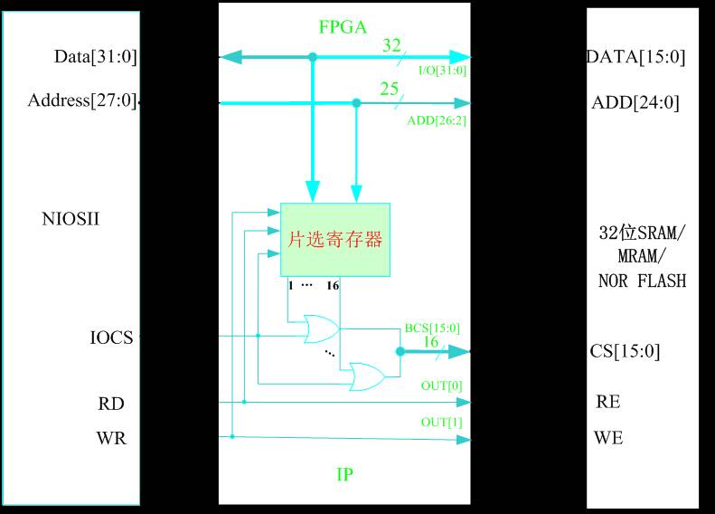
Figure 43: 32-bit SRAM/MRAM/NOR FLASH Interface IP
Design of 40-bit SRAM/MRAM/NOR FLASH Interface IP Core
As shown in Figure 4-4, the 40-bit data width is somewhat special. Here, we divide the 40-bit data into five 8-bit areas, using an 8-bit wide bus to access each area separately. The bit selection register in the IP core is used to switch the 8-bit data bus to one of the five areas of the 40-bit bus. The address of the chip select register is (base address + 0x0FFFFFFC), and the address of the bit selection register is (base address + 0x0FFFFFF8). The maximum testable memory module is 128M×40 bits×16 chips for SRAM/MRAM/NOR FLASH.
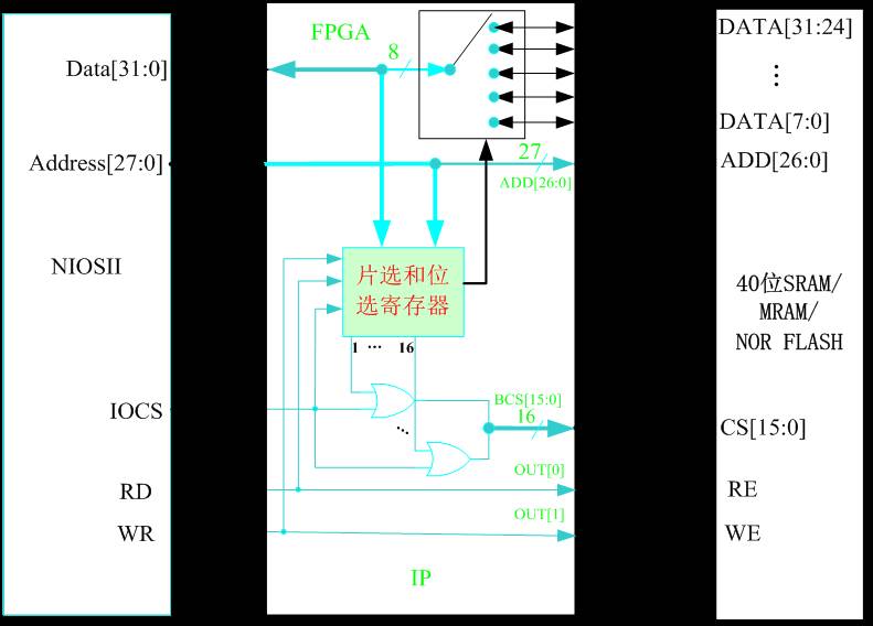
Figure 44: 40-bit SRAM/MRAM/NOR FLASH Interface IP
Design of 8-bit NAND FLASH ABUS Interface IP
As shown in Figure 4-5, by writing to the chip select register, one of the 16 chip selects of the module can be selected. We agree that its address is (base address + 0x0FFFFFFC). The read status register returns the busy signals of the 16 NAND FLASH chips, with its address being (base address + 0x0FFFFFF8). Writing data to address (base address + 0x00) is a write operation to the NAND FLASH data register. Reading data from address (base address + 0x00) is a read operation from the NAND FLASH data register. Writing data to address (base address + 0x01) is a write operation to the NAND FLASH command register. Writing data to address (base address + 0x02) is a write operation to the NAND FLASH address register.
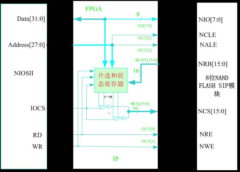
Figure 45: Design Diagram of 8-bit NAND FLASH ABUS Interface IP Core
Design of 16-bit NAND FLASH ABUS Interface IP
The 16-bit NAND FLASH memory chip can have multiple combination methods, either using multiple 16-bit NAND FLASHs or multiple 8-bit NAND FLASHs. Here, we assume that the 16-bit SIP NAND FLASH product is made up of multiple 16-bit NAND FLASH chips, and the following IP core is designed based on its structure.
As shown in Figure 4-6, by writing to the chip select register, one of the 16 chip selects of the module can be selected. We agree that its address is (base address + 0x0FFFFFFC). The read status register returns the busy signals of the 16 NAND FLASH chips, with its address being (base address + 0x0FFFFFF8). Writing data to address (base address + 0x00) is a write operation to the NAND FLASH data register. Reading data from address (base address + 0x00) is a read operation from the NAND FLASH data register. Writing data to address (base address + 0x01) is a write operation to the NAND FLASH command register. Writing data to address (base address + 0x02) is a write operation to the NAND FLASH address register.
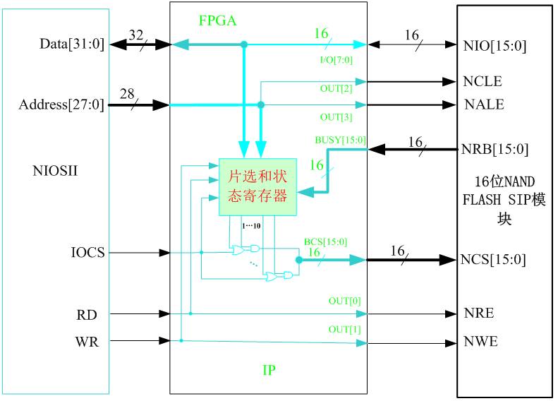
Figure 46: Design Diagram of 16-bit NAND FLASH ABUS Interface IP Core
Verification and Conclusion
After writing the programmed FPGA and debugging the C code into FLASH, reconfiguring the FPGA after power loss allows the serial port output to correctly identify all the configured memory chips and accurately perform read/write functional tests, achieving the design objectives.
This paper introduces a low-cost, simple, and flexible hardware design for a multifunctional memory chip testing system, utilizing FPGA, FLASH, SDRAM, RS232 circuits, etc. By adopting this scheme, users can flexibly add testing system functions according to market demands, achieving more memory chip testing.
References:
[1] K9F4G08U0B 512M x 8 Bit / 1G x 8 Bit NAND Flash Memory datasheet, May 30, 2008
[2] Avalon Interface Specifications, Version 1.3, August 2010
[3] R1RP0416D Series 4M High Speed SRAM datasheet, Rev. 1.00, Mar. 12, 2004
[4] HN58V1001 Series 1M EEPROM datasheet, Rev. 7.0, Oct. 31, 1997
[5] MR0A08B 128K x 8 MRAM Memory datasheet, Rev. 2, 6/2009
[6] S29JL064H 64 Megabit (8 M x 8-Bit/4 M x 16-Bit) datasheet, Revision A, March 26, 2004