
1. What is PCB Silk Screen Printing?
PCB silk screen printing mainly refers to text-based information, including circuit points, components, circuit symbols, etc. The silk screen signals vary according to the size of the PCB. If space is limited, the most critical information must be prioritized.

Silk screen printing on PCB
PCB silk screen printing mainly includes the following:
-
Component reference designators
-
Polarity markings
-
Pin 1 markings
-
Component boundaries
-
Company logos
-
Manufacturer markings
-
Warning symbols
-
Part numbers
-
Version numbers
-
Date codes
PCB silk screen diagram
2. Complete Process of PCB Silk Screen Printing
1. Design the silk screen
Use EDA software to design the silk screen layer. This includes identifying and assembling all necessary markings, symbols, and text required for components on the PCB. Then export in a format usable by the manufacturer.
PCB silk screen diagram
2. Manufacture the PCB
The PCB manufacturing process includes printing a layer of copper on the substrate, drilling holes for components, and then etching away excess copper to create the PCB, which may have different shapes and patterns.
Use a specialized silk screen printing process to print the silk screen on top of the copper layer.
3. Apply silk screen printing
After the PCB is manufactured, use the silk screen printing process to print the silk screen layer, which involves creating a template for the silk screen design. This is done by applying a photosensitive emulsion to the mesh to create a template of the desired image.
4. Cure the ink
After applying the silk screen layer, the ink must be cured to ensure it adheres properly to the PCB substrate, typically by exposing the PCB to high temperatures or ultraviolet light for a specified time.
5. Inspect and test the PCB
Finally inspect and test the PCB to ensure the silk screen layer is applied correctly and that all necessary markings and symbols are printed. Errors and omissions in silk screen printing can lead to assembly errors or functionality issues.
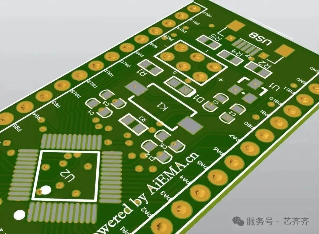
See the image below, which shows a 3D view of a PCB with silk screen:
3D view of a PCB with silk screen
The following is a 3D view of a PCB without the silk screen layer
One can compare the difference, thus ensuring the PCB has correct markings for easy identification, thereby reducing the risk of errors during assembly and improving the overall reliability of the finished product.
3. PCB Silk Screen Design
Here are some considerations for PCB silk screen design:
1. Component orientation and polarity
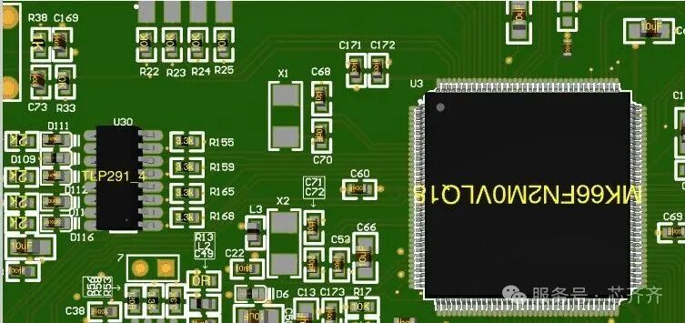
The direction marked on the silk screen indicates the orientation for soldering components, usually indicated by a dot, marking pin 1 of the IC.If it is an LED or diode, it will be marked with “+” or “C”, where C is the cathode and A is the anode.If it is a capacitor, a half-shadowed circle indicates negative polarity, while “+” indicates positive polarity.
PCB silk screen
2. Direction overlap
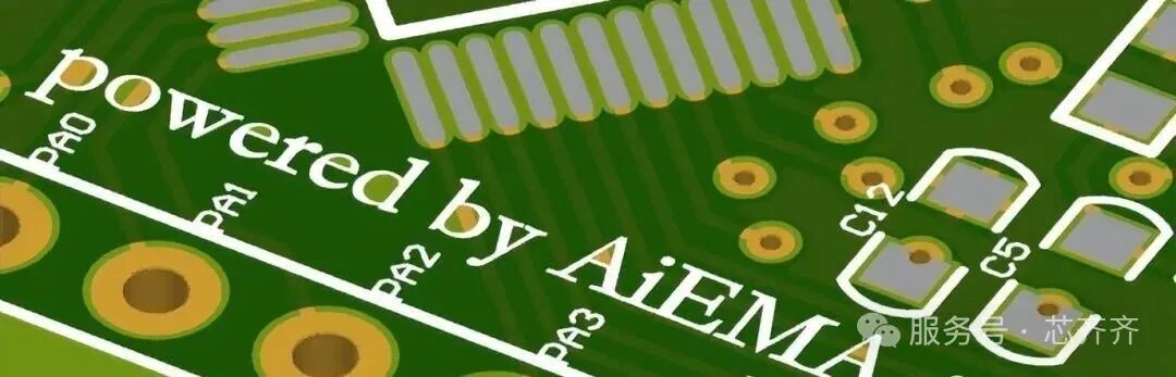
Edit the text direction of component reference designators, part types, etc., ensuring they are all in one direction for easy reading, and you can set silk screens for both the top and bottom.
Before rotating text and adjusting component reference indicators, check for text overlap. As shown in the figure below, the marked directions are inconsistent and overlap. During assembly and troubleshooting, they cannot be used as a reference. Therefore, during design, if such overlapping occurs, it is necessary to rotate the corresponding components and move the reference indicators to the correct direction and position.
Direction overlap
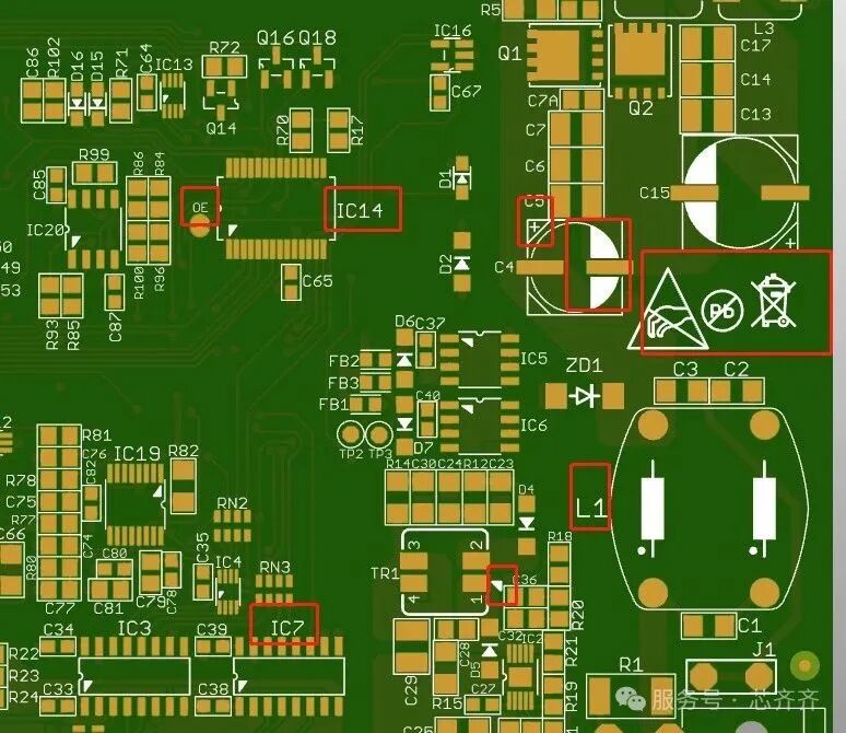
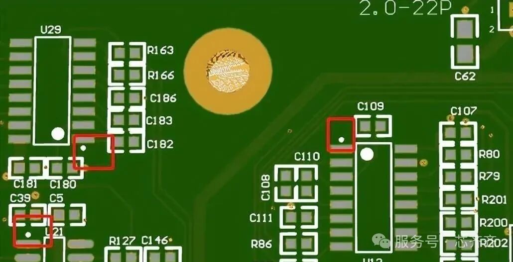
Check whether the component reference indicators placed on the PCB pads overlap with the pads. As shown in the first marked indicator in the figure below, it overlaps with the pad, making it impossible to use as a reference during assembly and troubleshooting. Therefore, the indicator needs to be moved to a blank position corresponding to the component.
Component reference overlapping with pads
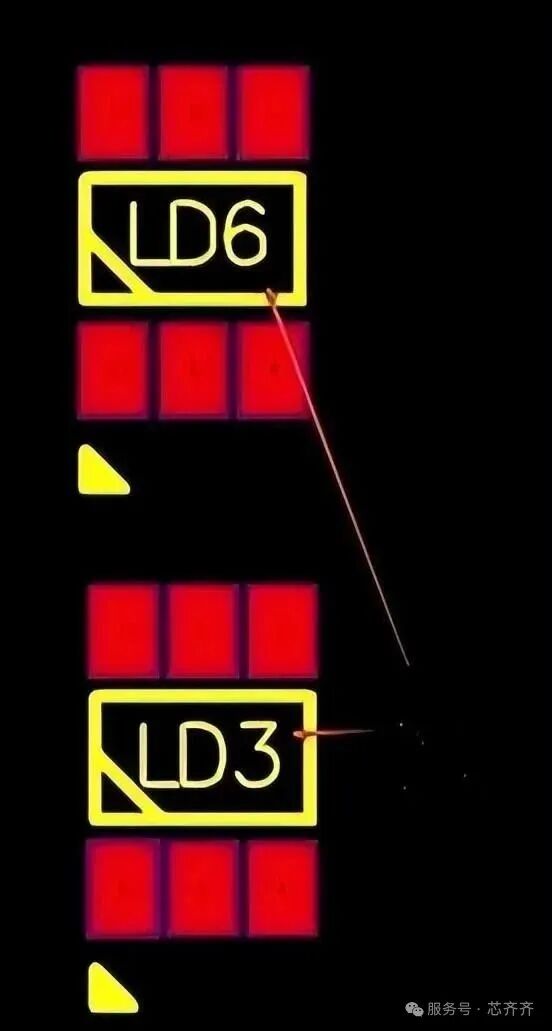
Check the markings on the vias. As shown in the second component marking in the figure below. Since non-tented vias cannot be printed, when you use a solder mask to cover the tented vias, it cannot be used as a test point, and it is best to move it next to the component.

Check the markings on the vias
Check whether reference markings are placed so that the reference markings are located below the soldered components. If, as shown below, there is a marking below the component, it should be moved to a blank position next to the component.
Reference marking is not visible
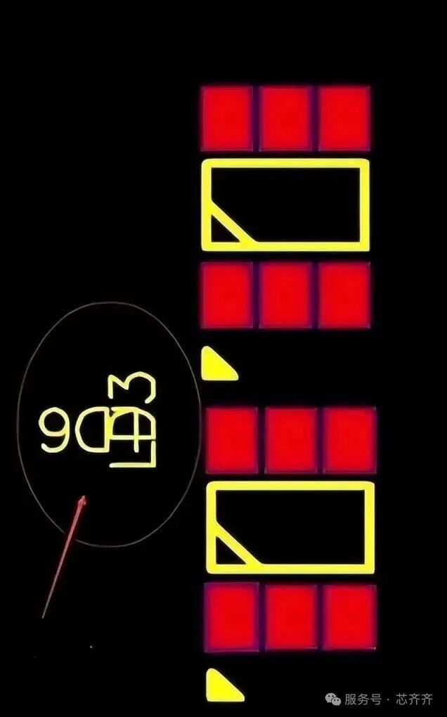
3. Additional markings
Adding extra markings can better indicate the orientation of components. For example, in the figure below, in addition to the original marking direction of the component, you can add triangular, circular, or other shapes to indicate the direction of I/O components.
Silk screen markings
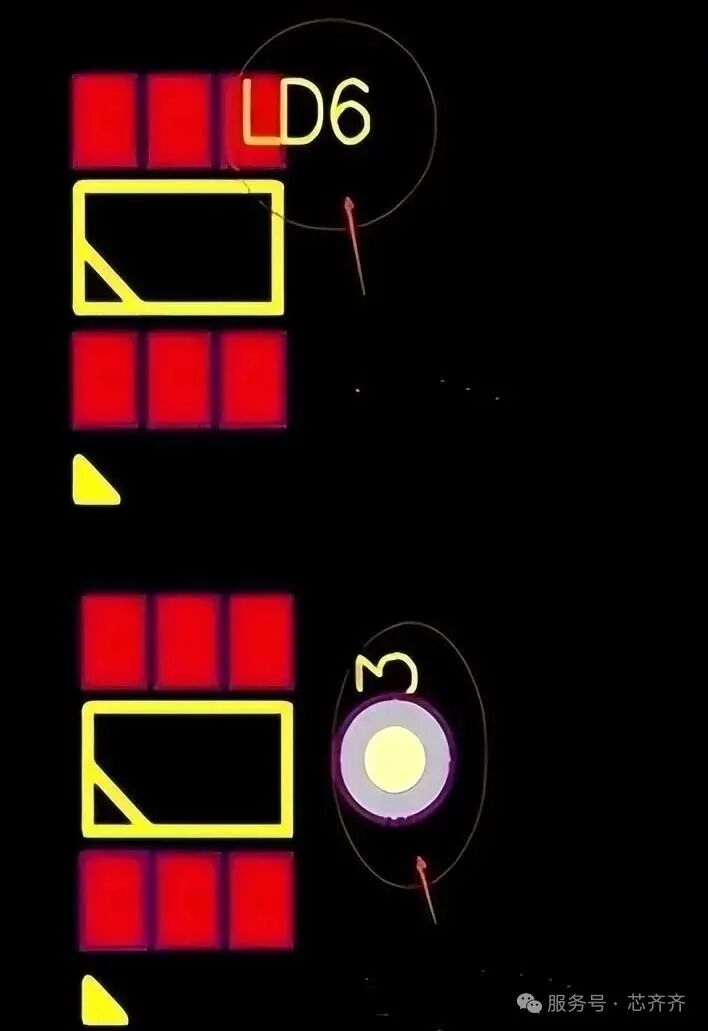
Place polarity markings outside the component object markings, as shown in the figure below for positive polarity markings, which are generally required for polarized components such as electrolytic capacitors, diodes, and LEDs.

Polarity markings
Measurement markings for pin and line counts on ICs can also be added to the silk screen, as shown below:
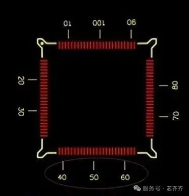
Measurement markings for pin and line counts on ICs
4. Silk Screen Printing Process
Selecting the appropriate silk screen printing process is very important, as the printing method will affect design parameters, such as the size, spacing, and position of silk screen printing on different component pads, traces, and vias.
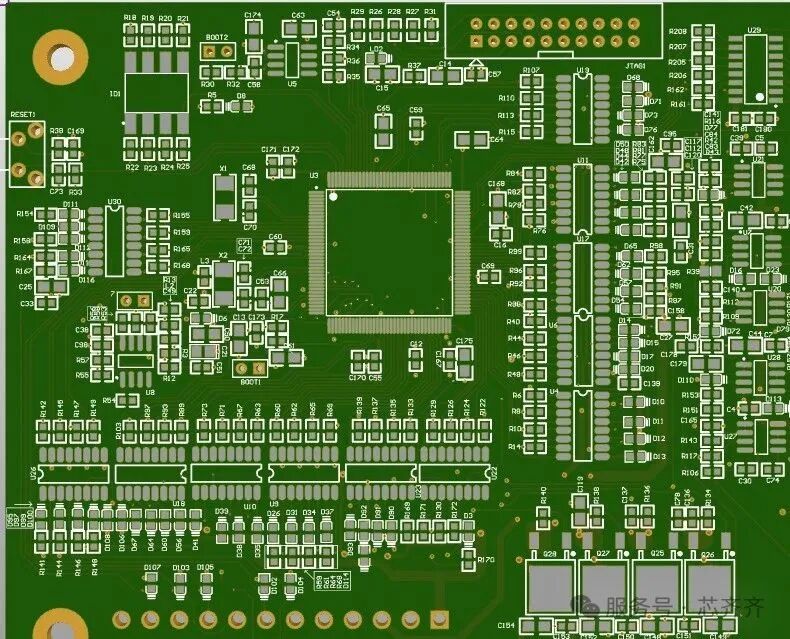
PCB diagram
5. Suitable Silk Screen Fonts
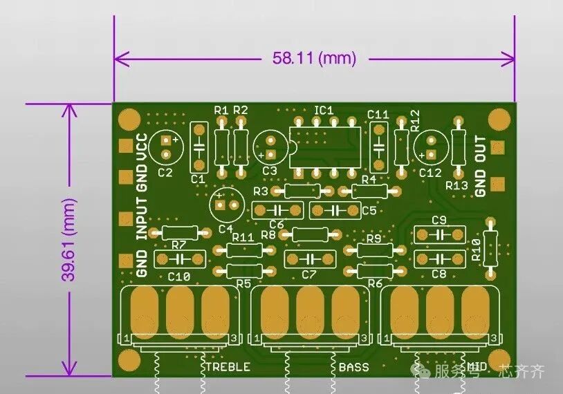
Selecting appropriate fonts is crucial for readability, such as the size, height, color, and font styles. The most common sizes are 35 mil height and 5 mil line width, as well as 25 mil height and 5 mil line width.
Suitable silk screen fonts

Some screenshots of electronic books

【Complete Set of Hardware Learning Materials】