Introduction
The Versal RF series SoC features high-resolution, multi-channel RF converters and low-latency processing technology, enabling simultaneous capture and analysis of wideband spectra.
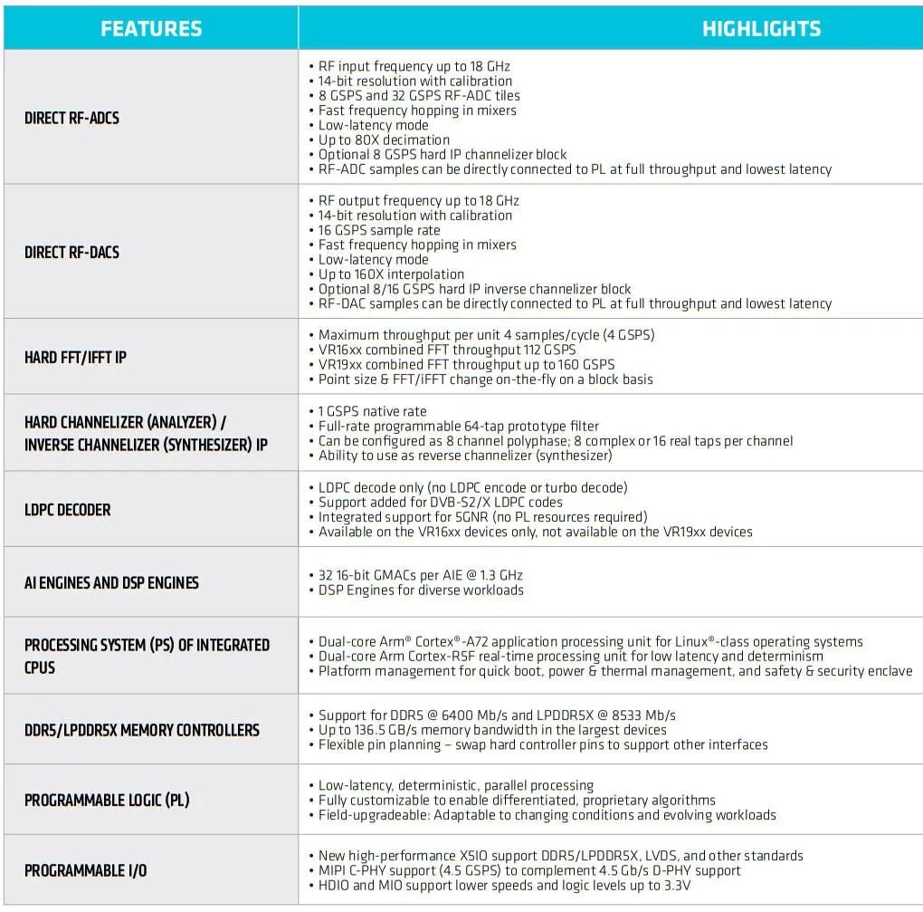
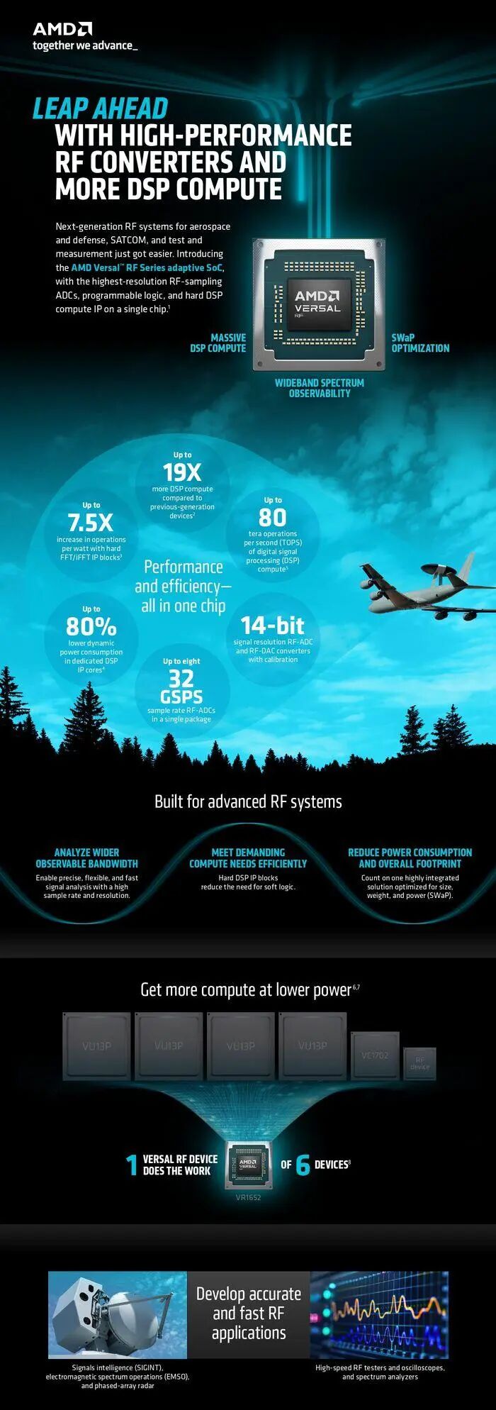
Its single-chip integrated 14-bit (after calibration) high-resolution, 32 GSPS sampling rate, 18 GHz RF analog-to-digital converter (RF-ADC) allows for precise, flexible, and rapid signal feature analysis across a wide observable spectrum, suitable for critical tasks such as phased array radar, electronic warfare, signal intelligence, and military and satellite communication terminals.
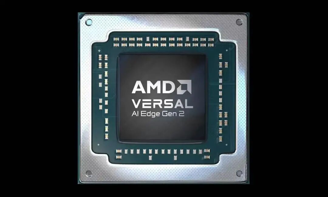
For T&M applications such as high-speed oscilloscopes, wideband spectrum analyzers, and signal generators, the Versal RF series provides highly integrated solutions, supporting RF channels up to the Ku band and advanced T&M signal processing functions such as arbitrary resampling and spectrum analysis. Direct RF sampling up to 18 GHz and sampling rates up to 32 GSPS enable digitization of several GHz of RF bandwidth across multiple channels simultaneously.
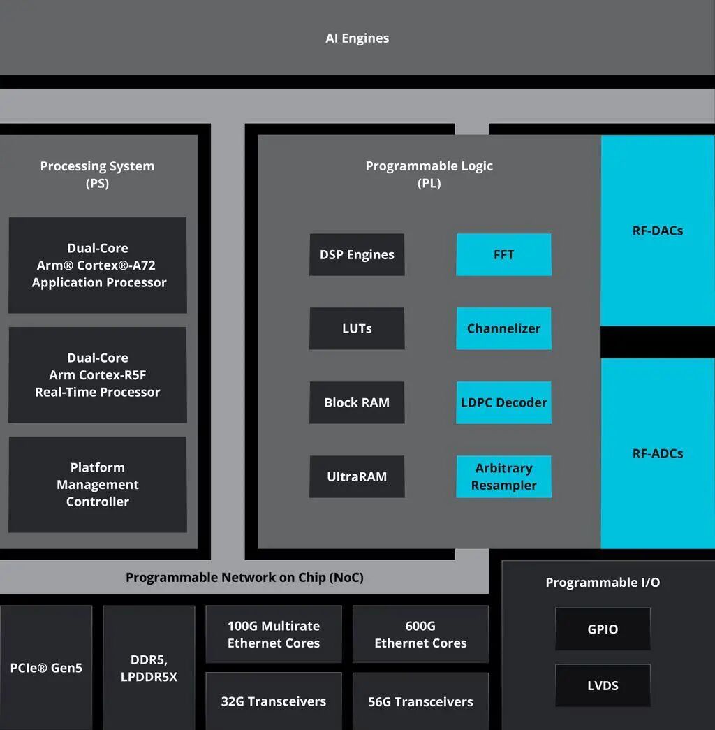
The Versal RF series offers up to 80 TOPS of DSP (digital signal processor) computing power, achieving up to a 19-fold increase in DSP performance in channelized mode compared to the current generation of AMD Zynq UltraScale+ RFSoC devices.
Some DSP functions are implemented through dedicated hardware IP modules, including 4 GSPS FFT/iFFT, channelizers, arbitrary resamplers, and LDPC decoders, achieving up to an 80% reduction in dynamic power consumption compared to AMD soft logic implementations.
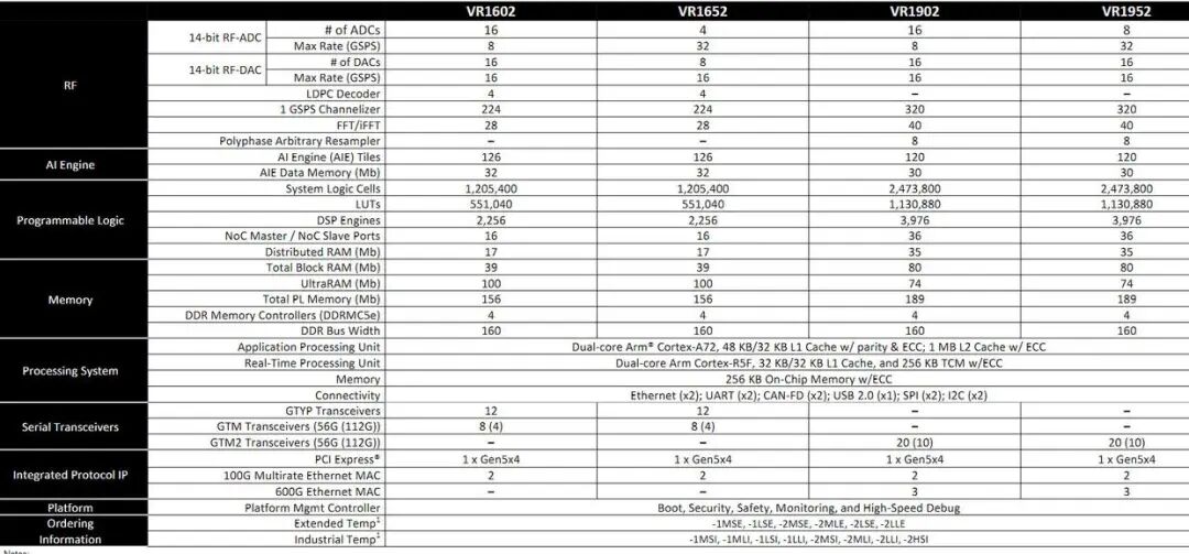
The Versal RF series development tools are now available. Silicon samples and evaluation kits are expected to be released in Q4 2025, with mass production anticipated to begin in the first half of 2027.
Versal is AMD’s (formerly Xilinx) adaptive computing acceleration platform series, designed for high-performance computing, AI acceleration, and embedded systems, integrating heterogeneous resources such as FPGAs, AI engines, and multi-core processors. Its core value lies in meeting diverse computing needs through a flexible hardware architecture and efficient on-chip communication mechanisms. Here are the key points:
System Architecture and Core Resources
Heterogeneous Computing Architecture: Versal adopts a ‘FPGA + ARM’ hybrid architecture, integrating programmable logic (PL), AI engines, and Arm processor systems (PS), supporting the collaboration of hardware acceleration and software control.
Key Hardware Units:
AI Engine: A computing array optimized for machine learning algorithms, providing high-throughput matrix computation capabilities.
Programmable Logic (PL): Traditional FPGA resources that support user-defined hardware acceleration circuits.
Processor System (PS): Includes dual-core Cortex-A72 (APU) and real-time processors, responsible for system control and general computing tasks.
High-Speed Interconnect (NoC): A 128-bit wide on-chip network that supports AXI protocol conversion, enabling low-latency data transfer across modules.
On-Chip Network (NoC) and Communication Mechanisms
NoC serves as the backbone for data flow, ensuring bandwidth allocation through predefined routing tables and QoS policies. Its features include:
Protocol Compatibility: Supports automatic conversion of AXI3/AXI4/AXI4-Stream interfaces.
Configuration Automation: Initialization is completed during the startup phase by the PMC controller via the NPI interface, requiring no manual intervention from users.
Extended Applications: AXI NoC IP simplifies the connection design between PL and DDR controllers and PS.
System Management and Boot Process
Platform Management Controller (PMC):
Responsible for core system services such as boot process (BootROM loading PLM firmware), power management, and security monitoring.
Integrates three types of flash controllers, supporting booting from NOR/NAND Flash or auxiliary interfaces (e.g., Ethernet).
Dynamic Reconfiguration: Supports Dynamic Function eXchange (DFX) technology for dynamic switching of hardware functions.
High-Performance Interfaces and Security Features
High-Speed I/O Subsystem:
Integrates Multi-Rate Ethernet MAC (MRMAC) supporting 100G Ethernet.
PCIe® CPM module provides DMA acceleration and cache coherence.
Security Enhancements: Built-in encryption engines (e.g., AES-256), root of trust mechanisms, and lifecycle management to meet functional safety standards.
Typical Application Scenarios
Data Center Acceleration: AI inference, video transcoding, and other scenarios accelerated through collaboration between AI engines and PL.
5G Communication: Utilizing MRMAC and low-latency NoC for base station signal processing.
Industrial Control: APU running Linux system control, PL handling real-time motion control algorithms.
This platform allows developers to deploy application software on the PS side and implement hardware acceleration on the PL side through a decoupled design (e.g., Vitis toolchain), significantly improving the development efficiency of complex systems.
Disclaimer:
This account maintains neutrality regarding all statements and views in original and reprinted articles. The articles are provided for readers’ learning and communication purposes. Copyright for articles, images, etc., belongs to the original authors. Some articles have unknown sources; if there is any infringement, please contact for deletion. For submissions/promotions, please add WeChat: 15989459034