
Source: Xilinx, cnbeta, AnandTech
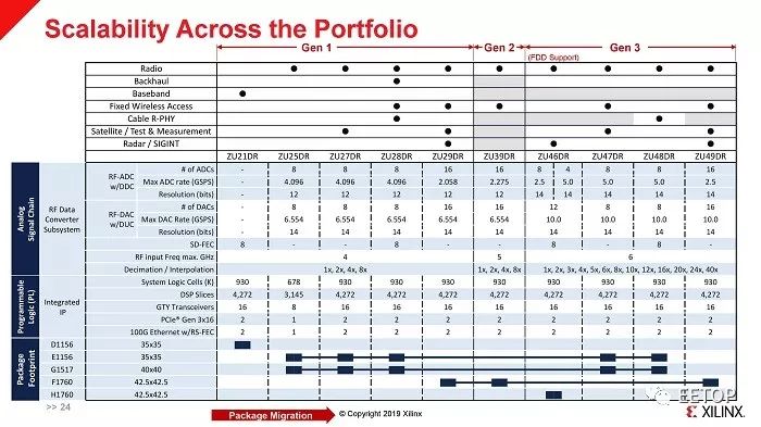
On February 21, 2019, Xilinx, a global leader in adaptive and intelligent computing, announced a new addition to its award-winning Zynq® UltraScale+™ RF system-on-chip (SoC) product line, featuring enhanced RF performance and greater scalability. The new generation of devices builds on the success of the Zynq UltraScale + RFSoC core product line across multiple markets, supporting all frequency bands below 6GHz to meet the critical demands of next-generation 5G deployments. It also supports direct RF sampling for 14-bit analog-to-digital converters (ADC) and 14-bit digital-to-analog converters (DAC) with sampling rates of up to 5GS/S, both with an analog bandwidth of up to 6GHz.

The Xilinx RFSoC product line is the only single-chip adaptive RF platform that meets current and future industry demands. This product line now includes:
-
Xilinx Zynq UltraScale + RFSoC Gen 2 (Second Generation): This device, which is now in sample availability and is planned for mass production in June 2019, is not only aligned with the timeline for 5G deployment in the Asia region but also supports the latest RF technologies.
-
Xilinx Zynq UltraScale + RFSoC Gen 3 (Third Generation): Compared to the core product line, it provides comprehensive support for direct RF sampling in the RF data converter subsystem for frequencies below 6GHz, extended millimeter-wave interfaces, and reduces power consumption by up to 20%. This product will be available in the second half of 2019.
The new single-chip integrates higher performance RF data converters, providing the necessary broad frequency coverage for deploying 5G wireless communication systems, cable television access, advanced phased array radar solutions, and other applications including measurement testing and satellite communications. By replacing discrete components, these devices can reduce power consumption and package size by 50%, making them an ideal choice for telecom operators deploying 5G systems for large-scale MIMO base stations.
Interpreting the Next Generation Zynq Ultrascale + RF SoC
Like the construction of 4G and 3G networks, the development of 5G networks requires the cooperation of many embedded wireless devices. Equipment manufacturers and testing platforms often cannot utilize all off-the-shelf components due to various system requirements, such as flexibility, density, rapid deployment, and reconfigurability. The good news is that Xilinx launched its next-generation Zynq Ultrascale + RF SoC yesterday, integrating digital hardware and analog modules into a single chip.
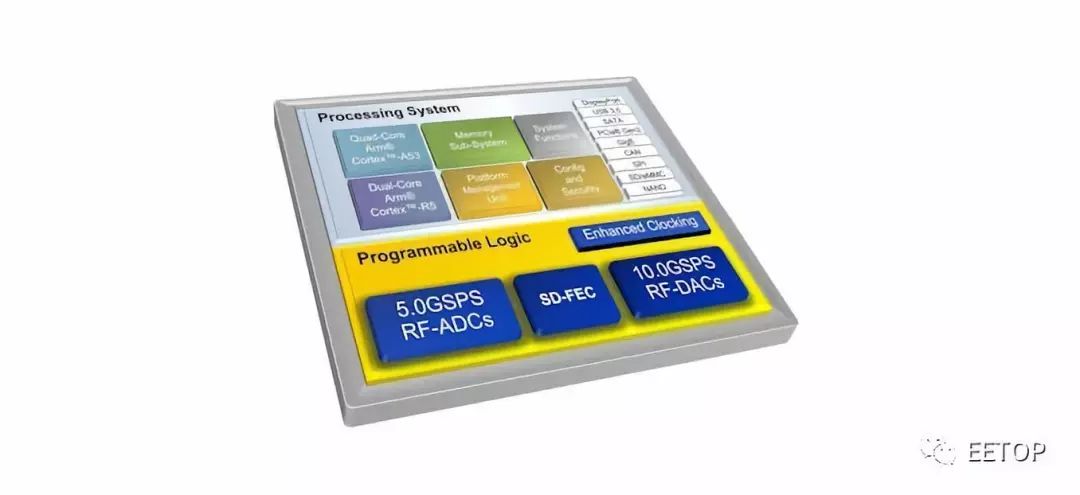
The RF SoC is a single-chip adaptive radio platform that integrates hardware, a programmable software engine, and RF analog technology densely, supported by TSMC’s 16nm process.
In previous generations of products, the system relied on multiple chips to perform all these tasks. But now, Xilinx offers an extremely simplified solution design that integrates a complete RF signal chain.
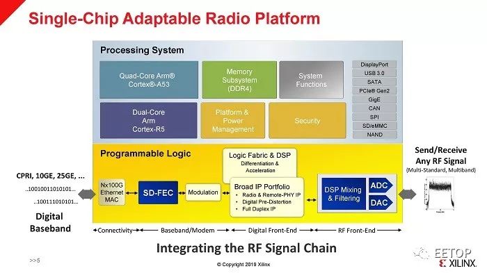
From MAC to DSP, wireless IP, baseband, modulation, DSP signaling and filtering, ADC/DAC, general-purpose digital processors, and DDR4 memory subsystems.
Xilinx states that one of the advantages of RFSoC is its focus on wireless networks’ Massive-MIMO RF modules.
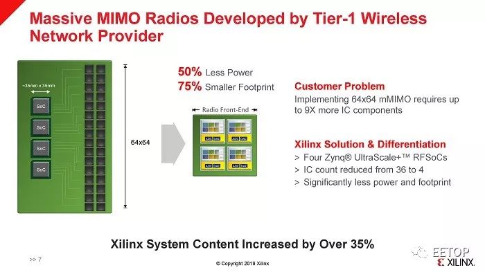
Xilinx introduced that with the help of RFSoC, 64×64 m-MIMO can reduce power consumption by half, installation amounts by 75%, and the number of system components by 89%.
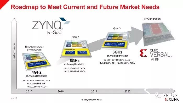
The newly released RFSoC products include the second and third generations. In the first-generation products, Xilinx provided solutions covering the 4GHz band and DOCSIS 3.1, achieving part of the positioning required for 5G deployment.
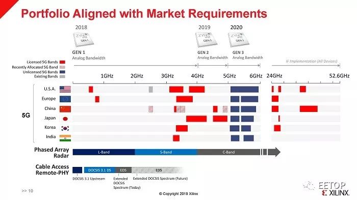
The second-generation product is a rapid strategic adjustment based on the first-generation fast market entry solution, covering the 5GHz band for quick deployment in markets such as China and Japan.
The third-generation product features a refreshed design that can cover the 6GHz band, supporting authorized and unlicensed spectrum, aimed at achieving global 5G deployment.
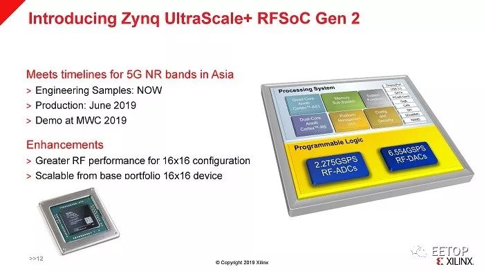
However, the first to hit the market will still be the second-generation product. As mentioned above, it is an enhanced version of the initial generation aimed at the Asian market, expected to begin testing under the 5G band soon.
Xilinx states that engineering samples are now available to specific customers and mass production will begin in June 2019. The third-generation product utilizes similar underlying hardware (quad-core A53 + dual-core A5 CPU with programmable logic).
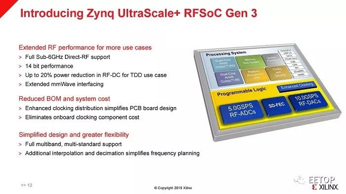
However, there are also upgrades for fixed-function ADC/DAC, as well as support for the 6GHz band across different clock domains, enhancing programmable logic clock, especially for the additional DSP requirements of 6GHz with up to 14-bit processing.
Xilinx states that the third-generation product will reduce power consumption on TDD, extend millimeter-wave interfaces, and support complete multi-band/multi-standard.
Enhanced clocks also mean that in external clock generator mode, the entire design only requires one external clock generator instead of up to four previously needed.
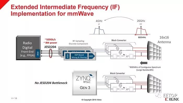
Xilinx states that its integrated analog/digital solutions also help implement intermediate frequency expansion in millimeter waves. A problem with traditional designs is that the RF sampling interface between discrete DSP and the digital front end is a given standard (i.e., JESD204).
However, in a 16×16 antenna scheme, the power consumption of this standard interface at 320 Gb/s is around 8W. If high-frequency spectrum of 800 MHz needs to be resolved, power consumption will increase significantly.
By integrating digital and analog components in the third-generation product, Xilinx can complete all interface work on a single chip, resulting in lower power consumption and faster transmission.
The company claims that Xilinx allows first-tier suppliers to use their custom programmable IP in conjunction with RF. Second-tier suppliers can also use proprietary or fixed IP solutions.
Through this design, Xilinx can add the RF market to its product portfolio. It is reported that the third-generation RFSoC will begin sampling in the second half of 2019 and start mass production in the third quarter of 2020.
As for why it took so long, it is because the supplier verification testing timetable took longer than we anticipated. This part will cover all unlicensed 6GHz and below frequency band chips.
It is worth noting that both the second and third generation devices will maintain pin compatibility with the first-generation hardware.