The quality of a PCB is not determined by how quickly it is laid out, but by whether you follow the “standardized design process”! This article will take you through the complete breakdown of the 22 standardized design steps, helping you avoid those frustrating rework issues!Clear thinking is far more important than hard work!
Many novice engineers often make the mistake of skipping the process and diving straight into the work, resulting in—rework, rework, and more rework! As shown in Figure 1, a standard PCB design flowchart helps you stay on track from the very first step.
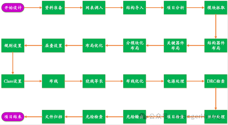 Figure 1: Standard PCB Design FlowchartStep 1: Data Preparation, Laying a Solid Foundation
The data that needs to be prepared before design includes:
-
The project’sfinal schematic
-
Package library or componentDatasheet
-
Structural DXF files with connector and height limitation information
-
Design specifications that clarifykey signals and chip requirements
-
Allimportant component datasheets
Step 2: Import Netlist, Ensure Accurate Connections
Import network connections and component packages from the schematic,and remember to synchronize the netlist once the schematic is updated!
Step 3: Import Structure, Avoid Crashes Later
Introduce structural board frames, positioning information, etc.,If the structure is updated, remember to re-import the DXF!
Step 4: Project Analysis Trio
Step 4: Project Analysis Trio
-
Schematic Block Diagram: Analyze functional modules
-
Design Specifications: Familiarize with key signal requirements
-
Power Binary Tree: Organize power branch flow (see Figure 2)
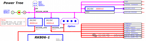
Figure 2: Power Binary Tree
Step 5: Functional Module Capture and Analysis
Capture components according to the schematic functional page, draw auxiliary lines in conjunction with modules, analyze signal flow, and assess board area in advance.
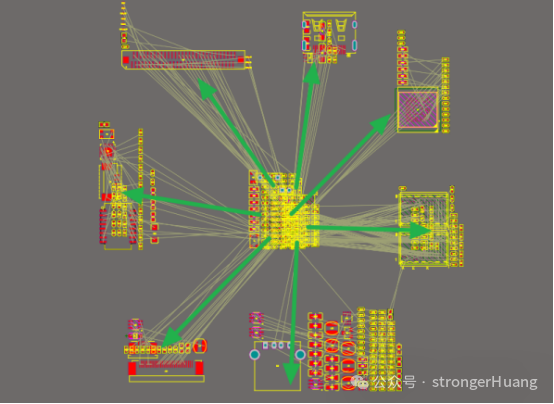
Figure 3: Module Division Illustration
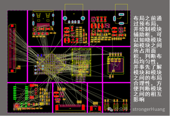
Figure 4: Signal Flow Analysis Diagram
Step 6: Structural Component Layout
According to the DXF structural file, import the board frame, and place components with positional requirements in the correct locations. If the structure is updated, remember to update it immediately to avoid repeating subsequent work.
Step 7: Key Component Layout
Place the main ICs in suitable positions on the PCB according to signal flow. This step is essentially the pre-layout of the PCB, which can effectively plan the overall signal flow and PCB layout density, improving layout rationality.
Step 8: Modular Layout
Individually layout the captured modules before placing them in suitable positions on the PCB. This part of the layout is detailed PCB layout, based on the pre-layout, following layout requirements and specifications. Please refer to the module specification requirements mentioned later, and pay attention to the position of holes and routing.
Step 9: Optimize Layout
Fine-tune the already laid-out components to make the entire PCB layout more reasonable and aesthetically pleasing.
Step 10: Layer SettingsBased on the flying wires after PCB layout, estimate the number of layers required for the design. According to the number of layers and board thickness, use stacking software (or existing stacking templates) to calculate the line width and spacing.Step 11: Rule Settings
Set line width and spacing rules on the PCB to facilitate routing. Rule settings need to check design requirements and the board factory’s process requirements; otherwise, it may lead to a complete re-routing.
Step 12: Class Settings
Group signals with design requirements according to IC signal requirements, set them into different classes, and establish corresponding class rules.
Step 13: Routing
Connect signals of the same network. After routing is completed, check the entire PCB routing requirements, inspect power routing to ensure it meets current carrying requirements and various certification requirements.
Step 14: Length Matching
Perform length matching for signals with timing requirements, paying attention to signal error requirements during matching.
Step 15: Routing Optimization
Optimize the already connected traces to make routing more aesthetically pleasing and reasonable. Focus on checking key signals and processing them optimally.
Step 16: Power Management
This step mainly optimizes power signals in the single board and divides power planes, confirming that they meet current carrying requirements. When dividing planes, ensure that important signal lines do not cross the division, as shown in the figure.
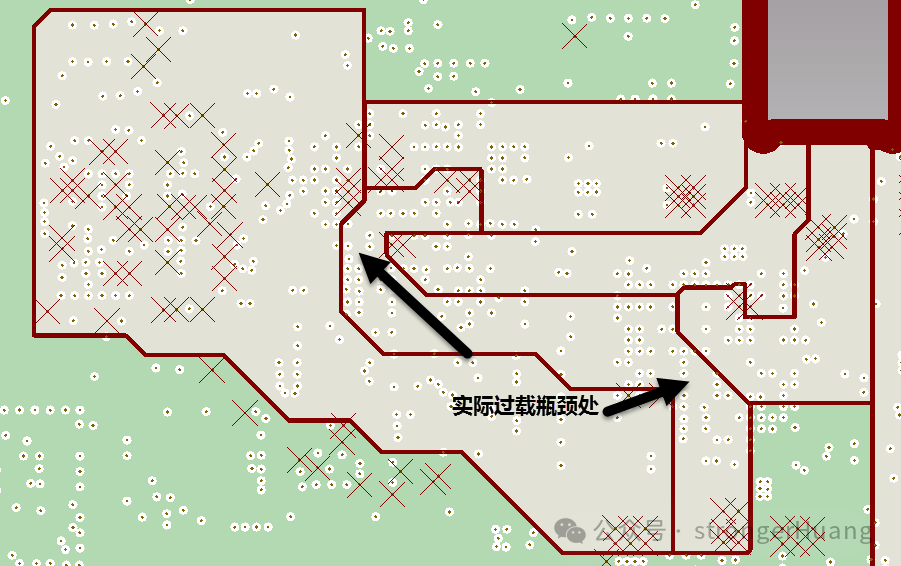
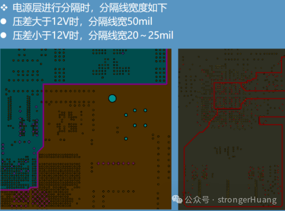
Figure 5: Division of Power Planes
Step 17: DRC Check1) Connectivity Check: Verify that all signals in the project are connected without open circuits;2) Other Checks: Check for short circuits in the project signals, avoid restricted areas, and avoid height limitations of components, etc.Step 18: Silkscreen Processing
Reasonably place component designators on the PCB, add corresponding version numbers, production identifiers (anti-static, SN number, company logo, etc.), ensuring that the silkscreen is easy to produce and readable.
Step 19: Project Review
Finally, double-check all customer design requirements and inspect manufacturability.
Step 20: Gerber Output
Set up and output Gerber files in EDA software. If it is a similar type of product, you can set up templates for Gerber output to facilitate one-click output during the next update.
Step 21: Gerber Check
Although EDA tools have effectively performed DRC checks on the designed PCB, the output Gerber should also be checked for manufacturability issues on some industry production tools. This can help resolve production issues during the design phase. Tools like Huachiu DFM are recommended for checking the output Gerber files.
Step 22: File Archiving
A good design file archiving can help us effectively improve communication and data transfer between departments and sections. Based on experience, it is recommended that designers archive files as follows:
1) ASM Folder: Contains assembly files, top and bottom assembly drawings, for customer assembly components → send to the SMT factory2) CAM Folder: Contains Gerber files, IPC netlist, PCB production instruction documents → send to PCB manufacturing factory or SMT factory3) DXF Folder: Contains structural drawing files used in the project → send to structural engineers4) PCB Folder: Contains the final PCB files of the project → for engineering designers to revise and design5) SCH Folder: Contains the final schematic files of the project → for engineering designers to revise and design6) SMT Folder: Contains SMT coordinate files and stencil files → send to the SMT factory
Summary:
The standardized process is not meant to increase workload, but toreduce rework and ensureefficient output. Whether you are a novice PCB designer or a seasoned hardware engineer,this 22-step process is your safeguard!
———— END ————

Latest Update on RT-Thread BSP Support List!

Step-by-step guide to understanding Keil MDK scatter loading files

Sharing an application running ROS on a microcontroller (RTOS)