What is a PCB Step Slot?
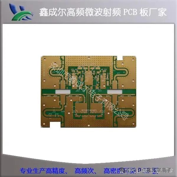
First, let’s briefly understand what a step slot is. In multilayer PCBs, conventional slots penetrate the entire thickness of the board. In contrast, a step slot is a non-through, depth-controlled slot that extends only to specific layers within the board, resembling a “step” in its cross-section, hence the name.
In high-frequency PCBs (which typically use special materials like PTFE/ceramic fillers), the creation of such step slots usually employs precision machining techniques such as controlled-depth milling or back-drilling.
Core Functions of Step Slots
Step slots play two key roles in high-frequency PCB design: controlling impedance and enabling three-dimensional interconnections.
1. Achieving Specific Impedance Control in Different Areas
Background:The quality of transmission for high-frequency signals (such as microwave and millimeter-wave) heavily depends on the characteristic impedance of the transmission line (typically 50Ω or 100Ω differential). Impedance is determined by factors such as dielectric thickness, trace width, and dielectric constant.
Function:By carving out step slots of varying depths in different areas, the dielectric thickness above the signal layer can be locally altered. For instance, in areas requiring more precise impedance control (such as antenna feed lines), a slot can be excavated to reduce the dielectric thickness between the signal line and the reference ground plane, allowing for wider traces to achieve the target impedance.
Why It Matters:Wider traces help reduce conductor losses (due to the skin effect), which is crucial for the integrity of high-frequency signals.
2. Creating Mounting Cavities for Surface-Mount Components
Background:Some components, such as chips, filters, and connectors, have a certain height. To reduce the overall profile height of the module and achieve a thinner design, components can be “embedded” within the PCB.
Function:Step slots can be precisely milled to create a recess for embedding components. This allows the top surface of the components to be nearly flush with the PCB surface, facilitating subsequent shield installation or achieving a flatter assembly.
3. Providing Shielded Cavities for RF Signal Vertical Transitions
Background:When signals need to transition vertically from the surface layer of the PCB to the bottom layer (or vice versa) through a coaxial connector, a reliable vertical interconnection structure is required.
Function:A ring-shaped step slot can be excavated around a metallized via (acting as a signal pin) and then metallized. This way, the metallized via (signal), the metallized slot wall (ground), and the dielectric in between form a miniature coaxial structure. This structure provides excellent electromagnetic shielding, minimizing signal energy leakage and mode conversion during vertical transitions, ensuring signal integrity.
Main Advantages of Step Slots
Based on the aforementioned functions, step slots provide significant advantages for high-frequency circuit design:
1. Enhanced High-Frequency Signal Integrity
Through precise impedance control and the creation of well-shielded vertical transitions, step slots effectively reduce signal reflections, attenuation, and crosstalk. This is essential for applications at millimeter-wave frequency levels.
2. Enabling Miniaturization and High-Density Integration of Systems
By embedding components within cavities, the Z-axis height of the module is significantly reduced, making devices (such as smartphones, drones, and phased array radar T/R modules) thinner and more compact.
3. Increased Design Flexibility and Performance
Designers are no longer constrained by uniform board thickness for impedance control. They can “customize” dielectric thickness in different areas of the board, finding the best balance between reducing losses and meeting structural requirements.
4. Improved Thermal Management and Mechanical Stability
When high-power devices are embedded within cavities, their bottoms may be closer to the copper layers or thermal vias inside the PCB, facilitating heat conduction.
The contact area between embedded components and the PCB is larger, and when combined with bottom-filling adhesives, it can provide a stronger mechanical connection than simple surface mounting, enhancing product reliability in vibration environments.
5. Cost Reduction (at the System Level)
Although the processing of step slots itself increases the manufacturing cost of the PCB, it may eliminate the need for external connectors, additional cables, or complex assembly structures, thereby reducing overall costs and assembly complexity at the system level.
Application Scenarios
Step slot technology is commonly found in fields with high performance and size requirements:
Phased Array Radar T/R Modules
* Base station antennas and millimeter-wave modules for 5G/6G communication
* Satellite communication equipment
* High-speed testing instruments and probe cards
* High-end aerospace and defense electronic systems
Conclusion
In summary, step slots on high-frequency PCBs are not just “slots”; they represent a precise “three-dimensional structural design.” By locally altering the physical structure of the PCB, they achieve precise control over electromagnetic fields and signal paths, making them one of the key technologies for addressing challenges in signal integrity, miniaturization, and integration in high-frequency circuit design. Their adoption reflects advanced capabilities in high-end high-frequency PCB design.