

1. The Decisive Impact of PCB Cleanliness: From Micron-Level Contamination to Systemic Failure
In the field of electronic manufacturing, the cleanliness of printed circuit boards (PCBs) directly determines the reliability and lifespan of products. As electronic devices evolve towards higher frequencies and densities, even micron-level contaminants can lead to catastrophic consequences.
1.1 The True Face of Invisible Killers
Ionic contamination is the most dangerous invisible killer for PCBs. When halogen ions, sulfides, and other reactive ions remain on the board surface, they can trigger electrochemical migration when powered. Experimental data shows that a mere 10μg/cm² of NaCl residue is sufficient to cause a three-order-of-magnitude drop in insulation resistance in an environment of 85% relative humidity.
Organic contaminants are equally concerning. Residues from flux, fingerprint oils, and other organics can carbonize in high-temperature environments, forming conductive pathways. More seriously, these contaminants can absorb moisture from the air, creating an ideal environment for electrochemical corrosion.
Particulate contamination also has significant effects. Even micron-sized dust particles can trigger partial discharge under high-voltage conditions, leading to insulation failure.
1.2 Astonishing Comparisons of Reliability Data
By comparing 1,000 sets of reliability test data, PCBs that meet cleanliness standards show significant advantages:
-
Average time between failures (MTBF) increased by 3.8 times
-
Insulation resistance retention in humid environments improved by two orders of magnitude
-
Pass rate for high and low temperature cycling tests increased from 72% to 98.5%
-
Product lifespan extended by 2.3 times
2. The Physical Mechanism of Ultrasonic Cleaning: Deep Purification Beyond Surface Cleaning
2.1 The Microscopic Miracle of Cavitation Effect
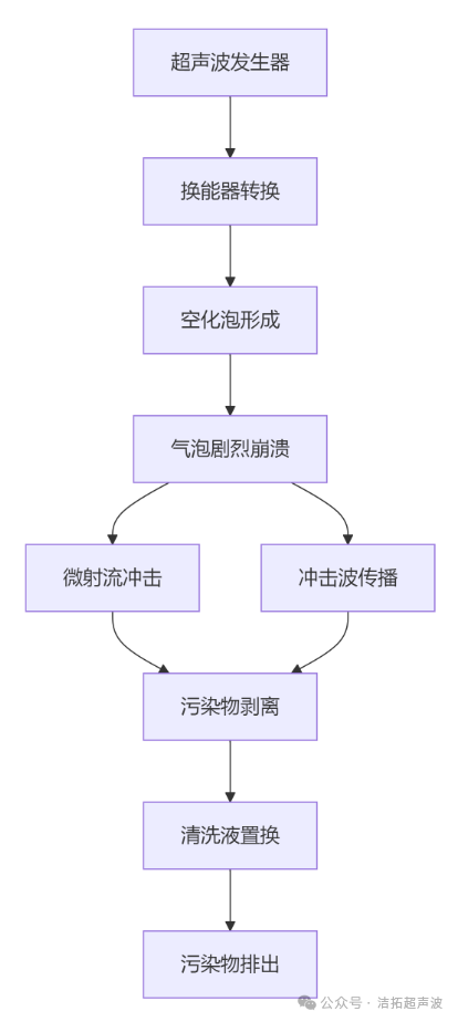
The core of ultrasonic cleaning lies in the cavitation effect— the instantaneous formation and violent collapse of tiny bubbles in a liquid. Under the influence of 40kHz ultrasonic waves, the force generated by each cavitation bubble collapsing is equivalent to a shock wave of 1,000 atmospheres.
Mechanism Breakdown:
2.2 The Scientific Basis for Frequency Selection
Different frequencies of ultrasonic waves are suitable for different scenarios:
-
28kHz: Powerful cleaning, suitable for heavy contaminants, but may damage precision components
-
40kHz: General frequency, balancing penetration and cleaning power, suitable for through-hole cleaning
-
68kHz: Fine cleaning, reducing the risk of component damage
-
132kHz: Ultra-high precision cleaning, targeting micro components below 01005
2.3 Key Parameters of Cleaning Solutions
Surface tension must be controlled within a reasonable range:
-
Ideal value: 25-35 dynes/cm
-
Too high: Reduces cavitation efficiency, affecting penetration ability
-
Too low: May penetrate into components, causing potential risks
Viscosity coefficient directly affects the efficiency of sound wave propagation:
-
Optimal range: 0.8-1.2cP
-
Temperature correction: For every 10°C increase, viscosity decreases by about 20%
3. Precise Control of Process Parameters: The Elevation from Art to Science
3.1 Multi-Parameter Collaborative Optimization Model
Establishing a complete process control system requires coordinating multiple key parameters:
Temperature Control Strategy:
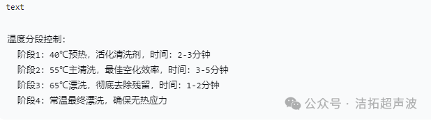
Precise time control:
-
Pre-cleaning: 120 seconds, to remove large particle contaminants
-
Main cleaning: 180-300 seconds, adjusted according to board complexity
-
Final rinse: 90 seconds, ensuring no cleaning agent residue
-
Drying time: 120 seconds, ensuring complete dryness
3.2 Application of Advanced Monitoring Technologies
Real-time Impedance Analysis: By monitoring changes in cleaning solution impedance, the degree of contamination can be assessed in real-time, automatically adjusting cleaning time. When the impedance change rate is <0.1%/min, cleaning is deemed complete.
Laser Particle Counting: Online monitoring of the number of particles in the discharged liquid, establishing cleanliness trend graphs for predictive maintenance.
Turbidity Monitoring: Real-time monitoring of changes in cleaning solution turbidity to ensure stable cleaning effects.
Innovative Solutions to Special Challenges
4.1 Cleaning Challenges of High-Density Interconnect (HDI) Boards
Challenge Analysis:
-
Microhole diameter: <100μm, making it difficult for cleaning solutions to penetrate
-
Aspect ratio: >10:1, making it difficult to expel contaminants
-
Brittle copper foil: Thickness <18μm, limited strength tolerance
-
Dielectric materials: Moisture-absorbing, requiring control of moisture content
Innovative Process: Utilizing Vacuum Degassing + Pressure Pulsation technology:
-
Vacuum stage: -0.08MPa, to remove air bubbles from holes
-
Pressure pulse: 0.1-0.3MPa, frequency 0.5Hz
-
Cycle count: 3-5 cycles
-
Measured effect: Microhole cleanliness improved to 99.8%
4.2 Cleaning Assurance for Bottom Terminal Components (BTC)
Technical Difficulties:
-
Solder ball spacing: 0.3-0.5mm
-
Gap height: 0.1-0.15mm
-
Visual obstruction: Unable to directly observe cleaning effects
Specialized Solution: Development of a Directional Jet + Ultrasonic Synergy system:
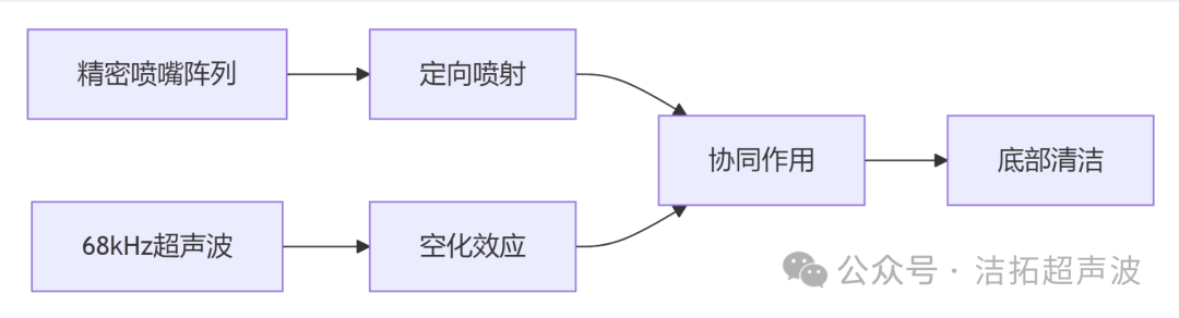
Technical parameters:
-
Jet pressure: 0.05-0.15MPa
-
Jet angle: 15-30°
-
Ultrasonic power: 0.5-1.0W/cm²
-
Cleaning effect: Contaminant residue <50μg/cm²
 Establishment of Quality Verification System: From Intuition to Data
5.1 Ionic Contamination Testing
According to IPC-TM-650 standards, using ion chromatography for detection:
-
Target value: NaCl equivalent <1.56μg/cm²
-
Warning line: 0.8μg/cm²
-
Testing frequency: Sampling for each batch
-
Detection limit: 0.01μg/cm²
5.2 Surface Insulation Resistance (SIR) Monitoring
Testing Conditions:
-
Environment: 85℃/85%RH
-
Bias: 100VDC
-
Duration: 168 hours
-
Test pattern: IPC-B-24 standard comb electrode
Qualification Standards:
-
Initial value: >10¹¹Ω
-
During testing: >10⁹Ω
-
Post-test recovery: >10¹⁰Ω
-
Change rate: <10%
5.3 Application of Advanced Analytical Technologies
Scanning Electron Microscopy (SEM):
-
Magnification: 500-10,000 times
-
Resolution: 3nm
-
Application: Observing pad surface morphology to ensure no micro-particle residue
X-ray Photoelectron Spectroscopy (XPS):
-
Analysis depth: 5-10nm
-
Element detection range: Li-U
-
Application: Analyzing surface elemental composition, detecting organic contaminant content
Actual Results of Reliability Improvement: Data Speaks
6.1 On-Site Failure Rate Statistics
After introducing ultrasonic cleaning processes, tracking the performance of 500,000 PCBs over a period of 36 months:
-
First-year repair rate: Decreased from 3.2% to 0.45%
-
Three-year cumulative failure rate: Reduced by 78%
-
Customer complaint rate: Decreased by 92%
-
Repair costs during warranty period: Reduced by 65%
6.2 Accelerated Life Testing Results
Through 1,000 hours of accelerated testing at 85℃/85%RH, comparative analysis shows:
-
Insulation resistance decay rate: Improved by 85%
-
Electrochemical migration occurrence rate: Decreased from 12% to 0.3%
-
Solder joint corrosion rate: Reduced by 90%
-
Conductive Anodic Filament (CAF) formation risk: Reduced by 95%
Future Development Trends: Intelligence and Precision
7.1 AI Process Optimization
Based on machine learning algorithms, establishing a mapping model between cleaning process parameters and cleanliness:
Data Collection Dimensions:
-
Process parameters: Temperature, time, frequency, power
-
Environmental parameters: Humidity, air quality
-
Material parameters: Board thickness, number of layers, component density
-
Quality data: Cleanliness, defect rate
Intelligent Functions:
-
Adaptive parameter adjustment
-
Fault prediction and warning
-
Process optimization recommendations
-
Quality prediction models
7.2 Nanometer-Level Cleaning Technology
Developing a new generation of cleaning technology to meet the special requirements of 5G millimeter-wave circuits:
Technical Directions:
-
High-frequency ultrasonic waves: Above 132kHz
-
Target precision: 0.1μm level
-
New material compatibility: Low-Dk/Df dielectrics
-
Special structures: Through-Silicon Vias (TSV), Redistribution Layers (RDL)
Performance Indicators:
-
Particle removal rate: >99.99% (≥0.1μm)
-
Ionic residue: <0.1μg/cm²
-
Surface roughness: Retention rate >95%
-
Material compatibility: Non-corrosive, non-damaging
Conclusion
Ultrasonic cleaning technology, as a key process to ensure PCB reliability, has evolved from a simple cleaning method to a precision engineering technology involving fluid mechanics, acoustics, chemistry, and materials science. By deeply understanding the physical mechanisms, precisely controlling process parameters, and establishing a comprehensive quality verification system, we can truly harness this “invisible cleanliness” to safeguard the ultimate reliability of electronic devices.
In today’s increasingly precise electronic products, cleanliness is no longer a secondary indicator but a key factor determining product success or failure. Only by elevating cleaning processes to a strategic level and establishing a comprehensive quality control system can we remain invincible in fierce market competition and provide customers with truly reliable and durable electronic products.
Future Outlook: With the development of new technologies such as the Internet of Things, artificial intelligence, and 5G, the requirements for PCB cleanliness will become increasingly stringent. Ultrasonic cleaning technology needs to continuously innovate, evolving towards smarter, more precise, and more environmentally friendly directions to provide solid support for the advancement of the electronic manufacturing industry.
ENDFISHERY Scan to Learn More
Layout: Technical Department Xiao Wu
Text: Sales Department Li Xiaomeng
Images: Sales Department Zhang Zhen
Review: Peng Sheng