Manufacturing Process of Multilayer PCBs

Manufacturing Process of Multilayer PCBs

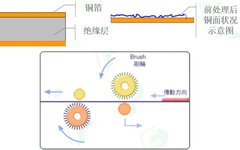
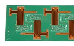
There are two methods for manufacturing multilayer boards: the electroplated via method and the high-density lamination method, both of which achieve circuit board structures through different combinations of processes. Currently, the most commonly used method is the electroplated via method, which has developed and improved over more than half a century. In terms of equipment, … Read more

Key Points in PCB Layout Design

Key Points in PCB Layout Design

In integrated circuit application design, after completing the project schematic design, PCB layout design is necessary. PCB design is a crucial step. The quality of the design results directly affects the overall functionality of the design. Therefore, a reasonable and efficient PCB layout is essential for the successful debugging of chip circuit design. In this … Read more

Analysis of Basic PCB Layout Principles

Analysis of Basic PCB Layout Principles

1.First, we will place the components that have structural requirements, paying attention to the placement position of pin 1 of the connector according to the imported structure. 2.During layout, attention should be paid to the height restrictions in the structure. 3.If you want the layout to be aesthetically pleasing, generally position components based on their … Read more

Top 10 PCB Tips from Industry Experts

Top 10 PCB Tips from Industry Experts

With the increasing integration of semiconductors, major electronic systems now feature complete system-on-chip designs and custom PCBs. It can be said that even an ordinary PCB can play a significant role, which sets high standards for engineers. This article summarizes the experiences of several experts and lists ten golden rules for PCB design, hoping to … Read more

Understanding How PCBs Work

Understanding How PCBs Work

1. Working Principle The working principle of a circuit board is to use an insulating material to separate the surface copper foil conductive layer, allowing current to flow along a pre-designed route through various components to perform functions such as work, amplification, attenuation, modulation, demodulation, and encoding. Figure 1: Circuit Board 2. Components The circuit … Read more

Understanding PCB Design Basics

Understanding PCB Design Basics

Quick PCB is dedicated to becoming the most influential training base for PCB design talent. Therefore, PCB Girl decided To launch a series of PCB design basic knowledge sharing on the Quick PCB Academy WeChat public account, along with project case analysis, to enable students to apply what they learn. To understand the knowledge related … Read more

Summary of PCB Process Design Experience

Summary of PCB Process Design Experience

Click Blue Text Follow us~ Today, I share an experience summary on PCB process design, hoping to inspire industry colleagues. 1 PCB Basic Technology 1.1 PCB Size and Shape The welding processing dimensions of the PCB material shape are width (200mm~250mm) * length (250mm~300mm). For PCBs with a long edge less than 125mm or a … Read more

15 PCB Failure Modes and Solutions

15 PCB Failure Modes and Solutions

Whether engineers or PCB manufacturers, they inevitably encounter PCB failures. The occurrence of these failures may lead to delays in product delivery, damage to the manufacturer’s reputation, and increased time and monetary costs. (Most importantly, it costs money.) Today, we mainly discuss PCB failure modes and solutions. (It is recommended to save for later viewing, … Read more

The Everlasting PCB: Comprehensive Analysis (Part One)

The Everlasting PCB: Comprehensive Analysis (Part One)

Before the advent of PCBs, circuits were made through point-to-point wiring. This method had low reliability, as aging circuits could lead to wire breakage, resulting in open or short circuits at connection points. Wire winding technology was a significant advancement in circuit technology, enhancing the durability and replaceability of wires by winding small diameter wires … Read more