With the development of the times, more and more people choose to become electronic engineers. When starting to learn PCB design, it is necessary to be exposed to a large number of technical terms and knowledge. This process must lay a solid foundation. This article will share ten industry terms, hoping to help everyone.
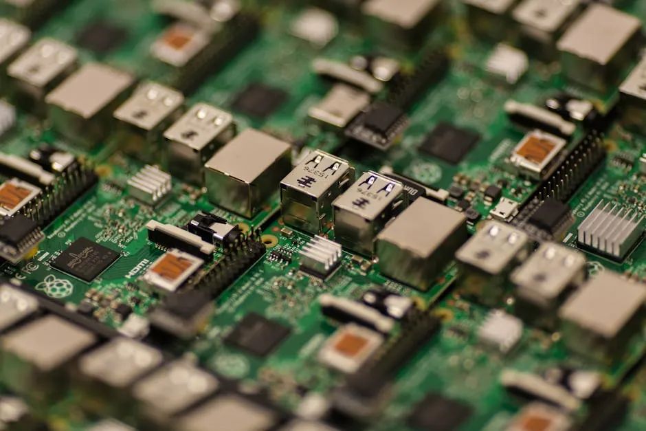
1. PCB PCB, or Printed Circuit Board, is an indispensable component in electronic devices. It carries various electronic components and provides electrical connections for these components. PCB is made using electronic printing technology, hence the name “printed” circuit board. On the PCB, wiring connects various electronic components to realize the function of the circuit;
2. SMT SMT, or Surface Mount Technology, is the mainstream technology in the electronic assembly industry today. It uses surface mounting to directly attach components to the PCB and fix and electrically connect them through soldering and other methods. SMT technology has advantages such as high assembly density and high production efficiency, and it is widely used in various electronic products;
3. PCBA PCBA is the final product of the assembled printed circuit board. It goes through processes such as SMT placement and DIP insertion, assembling various electronic components on the PCB to form a circuit module with specific functions. The quality of PCBA directly affects the performance and reliability of electronic products;
4. FPC Flexible Board FPC flexible board is a type of flexible circuit board characterized by its lightness and bendability. It is mainly used to connect other circuit boards or components to achieve the transmission of electrical signals. FPC flexible boards can be made into single-layer, double-layer, or multi-layer structures according to needs, adapting to different application scenarios;
5. HDI HDI, or High-Density Interconnect technology, is an advanced printed board production technology. It uses micro-blind buried hole technology to achieve high-density distribution of circuit board lines. HDI technology can improve the electrical performance and reliability of the circuit board while reducing product costs, suitable for high-performance, miniaturized electronic products;
6. PTH PTH, or Plated Through Hole, is a type of hole structure in printed circuit boards. It undergoes metallization treatment, making the inner wall of the hole conductive, thus achieving electrical connections between different layers of the circuit board. PTH holes have wide applications in circuit board design and are one of the key technologies for achieving multilayer circuit board interconnections;
7. Pad A pad is a conductive pattern on the printed circuit board used to connect component pins. It is usually located on the component mounting surface and corresponds to the component pins, achieving electrical connection through soldering and other methods. The shape and size of the pad need to be designed according to the specifications of the component pins to ensure the reliability and stability of the connection;
8. Package The package refers to the assembly pattern made on the printed circuit board according to the actual size and pin specifications of the component. The package pattern includes pads and surface silk-screening, guiding the installation and soldering of components. Correct package design can ensure the proper installation and stable operation of components on the circuit board;
9. Through Hole A through hole is used in printed circuit boards to connect electroplated pathways between different layers. It is usually used for inserting components, achieving electrical connections between component pins and the circuit board through soldering and other methods. The design of the through hole needs to consider factors such as hole diameter and hole position accuracy to ensure the reliability and stability of the connection;
10. DRC DRC, or Design Rule Check, is a program used to check whether there are errors in PCB design. After completing the PCB layout, DRC tools can be used for automatic checks to find omissions and errors, such as short circuits, overly thin traces, or holes that are too small. DRC checks help improve the accuracy and reliability of PCB design and reduce problems during the production process.
This article is an original article by Fany Enterprise Training, please indicate the source when reprinting!
Submission/Recruitment/Advertisement/Course Cooperation/Resource Exchange; please add WeChat: 13237418207