There are two methods for manufacturing multilayer boards: the electroplated via method and the high-density lamination method, both of which achieve circuit board structures through different combinations of processes. Currently, the most commonly used method is the electroplated via method, which has developed and improved over more than half a century. In terms of equipment, materials, and processes, the electroplated via method has matured and established a solid industrial foundation. The electroplated via method can be used to produce both double-sided and multilayer boards, with the processes and equipment being reusable. The electroplated via method involves plating a metal layer on the inner wall of the vias that penetrate the conductor patterns on the surface and inner layers of the insulating substrate, thus connecting the corresponding conductor patterns across different layers.
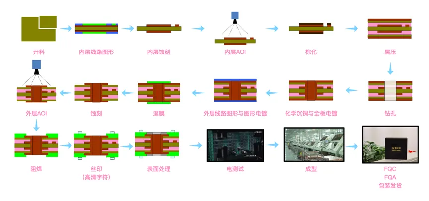
Taking the manufacturing process of a PCB factory as an example, the main manufacturing process for typical rigid multilayer boards is shown in the flowchart below:
The PCB factory does not directly manufacture copper-clad laminates, prepregs, copper foils, and other substrates, but purchases the required substrates from upstream substrate manufacturers in the supply chain. The substrates are typically supplied in standard large sizes, such as 1m*1m (or 1m*1.2m) specifications. Before PCB manufacturing, these substrates need to be cut into sizes suitable for the production line according to the specifications of the processing equipment.
After cutting the materials, the process for multilayer boards begins with the inner layer circuits, such as inner layer pattern production, lamination, etc. The process then returns to the same flow as that for double-sided boards, including drilling, plating, outer layer pattern production, and finally various inspections and packaging for shipment.
Inner Layer Pattern Production
The inner layers of multilayer boards typically use thin double-sided copper-clad substrates. After forming the inner layer circuits on the surface, lamination is performed to obtain the multilayer board.
A photosensitive dry film is adhered to the double-sided copper-clad board of the inner layer, followed by applying a film with the inner layer circuit pattern and exposing it. After exposure, development is carried out, and then the unnecessary copper foil is removed using an etching machine.
Once etching is complete, the inner layer circuits are revealed. At this point, it is necessary to remove the protective film that protects the circuits from etching, which is known as the film stripping process.
Next is the inspection of the inner layer, which is performed using Automatic Optical Inspection (AOI). Before lamination, to enhance the bonding strength between the copper foil and the prepreg, a browning treatment is required.
The purposes of browning are as follows:
1. Increase the contact area between the copper foil and the resin, enhancing the bonding strength between them;
2. Improve the wettability of the copper surface with the flowing resin, allowing the resin to flow into all corners for stronger adhesion after curing;
3. Generate a dense passivation layer on the copper surface to prevent the hardener from reacting with the copper under high temperature and pressure, which could produce water and cause board explosion.
The inner layers will be stacked according to the designed stacking structure, with the prepared inner layers, prepregs, and outer copper foils stacked in order, and then hot-pressed to form a single unit.
After lamination is complete, the process for producing the outer layer circuits begins, which is consistent with the process for double-sided boards.
After the PCB is laminated, the layers have not yet formed interconnections. At this point, drilling is required, followed by creating conductive copper layers on the hole walls to achieve interconnections.
Chemical Copper Deposition and Full Board Plating
Chemical copper deposition involves using chemical methods to deposit a thin layer of copper on the insulating hole walls, while full board plating is performed on the already chemically deposited, conductive hole walls to increase the copper thickness. This mainly includes three processes: glue residue removal, chemical copper deposition, and copper plating.
Glue residue removal clears the glue residue from the holes while simultaneously creating a micro-rough surface on the hole walls to enhance the bonding strength between the copper and the resin. Chemical copper deposition forms a thin metal layer on the hole walls, serving as a seed layer for plating. The plating process is intended to increase the copper thickness on the hole walls. Since there are no circuit patterns on the board surface at this stage, this step is referred to as “full board plating“.
Outer Layer Circuit Pattern
The purpose is to transfer the outer layer circuit to the copper-clad board throughout the process.
The purpose of pattern plating is to electroplate a layer of copper and tin to the required thickness on the exposed copper skin or hole walls of the circuit pattern.
The purpose is to remove the electroplating resist layer using NaOH solution, exposing the non-circuit copper layers.
The purpose of etching is to use chemical reactions to corrode the copper layers in non-circuit areas.
The main function of the PCB is to support and connect electronic components. After pattern plating, non-contact or soldering areas need to be protected with materials to prevent damage or oxidation. Solder paste is commonly used for component assembly, and these coated polymers are referred to as “solder masks”.
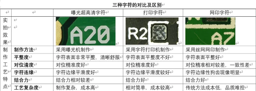
The purpose of characters is to provide recognizable markings.
This process differs from the “solder mask” process above; here, the areas that need to be soldered or contacted are protected to prevent the exposed copper foil from oxidizing upon contact with air, which could lead to poor soldering or contact issues.
The purpose is to punch or mill the required shapes using molds or CNC milling machines. Shaping methods include mechanical milling, punching, hand milling, and hand cutting.
Note: CNC milling and punching have higher precision, followed by hand milling, while hand cutting has the lowest precision and can only be used for simple shapes.
The purpose is to detect functional defects such as open circuits and short circuits that are not easily visible through electronic testing.
The purpose is to inspect the product for external defects and repair minor defects to prevent non-compliant products from being released.
Source: Wu Chuanbin’s Blog
Copyright Notice: This article is copyrighted by the original author and does not represent the views of the association. Articles promoted by the “Jiangxi Province Electronic Circuit Industry Association” are for sharing purposes only and do not represent the position of this account. If there are copyright issues, please contact us for deletion.