Analysis of Basic PCB Layout Principles

Analysis of Basic PCB Layout Principles
1.First, we will place the components that have structural requirements, paying attention to the placement position of pin 1 of the connector according to the imported structure.
2.During layout, attention should be paid to the height restrictions in the structure.
Analysis of Basic PCB Layout Principles Analysis of Basic PCB Layout Principles
3.If you want the layout to be aesthetically pleasing, generally position components based on their outer frame or central coordinate (center-aligned).
Analysis of Basic PCB Layout Principles
4.The overall layout should consider heat dissipation.
Analysis of Basic PCB Layout Principles
5.During layout, it is necessary to consider the evaluation of wiring channels and the space required for equal lengths.
Analysis of Basic PCB Layout Principles
6.During layout, it is necessary to consider the power flow direction and evaluate the power channel.
Analysis of Basic PCB Layout Principles
7.High-speed, medium-speed, and low-speed circuits should be separated.
Analysis of Basic PCB Layout Principles
8.High current, high voltage, and strong radiation components should be kept away from low current, low voltage, and sensitive components.
Analysis of Basic PCB Layout Principles
9.Analog, digital, power, and protection circuits should be separated.
Analysis of Basic PCB Layout Principles
10.Interface protection devices should be placed as close to the interface as possible.
Analysis of Basic PCB Layout Principles
11.The sequence of interface protection devices is required:
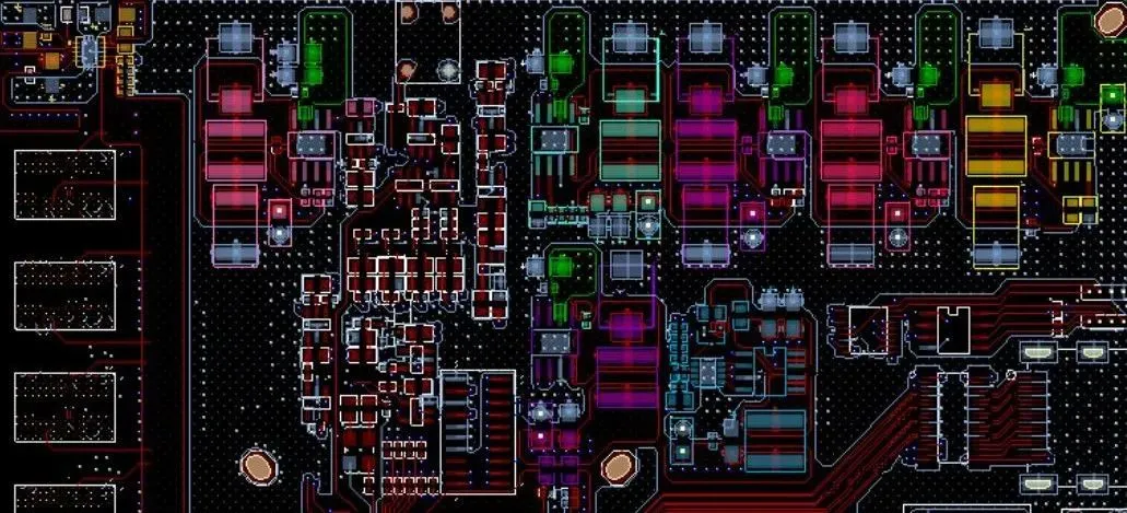
  • The typical sequence for power surge protection devices is: varistor, fuse, suppression diode, EMI filter, inductor or common mode inductor. For any missing components in the schematic, layout them sequentially.
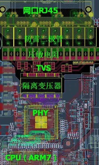
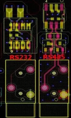
  • The typical sequence for interface signal protection devices is: ESD (TVS diode), isolation transformer, common mode inductor, capacitor, resistor. For any missing components in the schematic, layout them sequentially, strictly according to the schematic order (ability to judge the correctness of the schematic is required) in a “linear” layout.
Analysis of Basic PCB Layout Principles
12.Level shifting chips (such as RS232) should be placed close to the connector (such as serial port).
Analysis of Basic PCB Layout Principles
13.Devices that are susceptible to ESD interference, such as NMOS and CMOS devices, should be kept away from areas prone to ESD interference (such as the edges of the PCB).
Analysis of Basic PCB Layout Principles
14.Clock device layout:
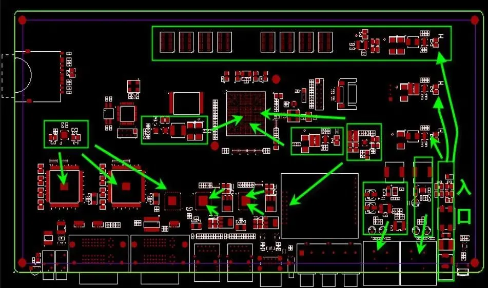
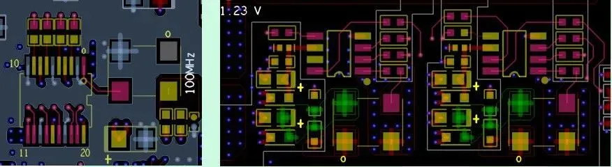
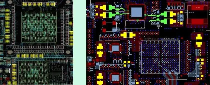
  • Crystals, oscillators, and clock distributors should be placed as close as possible to the relevant IC devices;
  • The filter for the clock circuit (preferably use a “∏” type filter) should be close to the power input pin of the clock circuit;
  • Check if there is a 22-ohm resistor in series with the output of the oscillator and clock distributor;
  • Check if the unused output pins of the clock distributor are grounded through a resistor;
  • The layout of crystals, oscillators, and clock distributors should be kept away from high-power components, heat sinks, and other heat-generating devices;
  • Check if the distance from the crystal oscillator to the board edge and interface devices is greater than 1 inch.
Analysis of Basic PCB Layout Principles
15.Switching power supplies should be kept away from AD/DA converters, analog devices, sensitive devices, and clock devices.
Analysis of Basic PCB Layout Principles
16.Switching power supply layout should be compact, with input/output separated, and layout should be strictly according to the schematic requirements, without randomly placing the capacitors of the switching power supply.
Analysis of Basic PCB Layout Principles
17.Capacitors and filter devices:
  • Capacitors must be placed close to the power pins, and the smaller the capacitance value, the closer it should be to the power pins;
  • EMI filters should be close to the power input of the chip;
  • In principle, each power pin should have a 0.1uF small capacitor, and each integrated circuit should have one or more 10uF large capacitors, which can be adjusted according to the specific situation.
Analysis of Basic PCB Layout Principles

Copyright Notice: This article is copyrighted by the original author and does not represent the views of the association. Articles pushed by the “Jiangxi Province Electronic Circuit Industry Association” are for sharing purposes only and do not represent the position of this account. If there are copyright issues, please contact us for deletion.

Analysis of Basic PCB Layout Principles

Leave a Comment