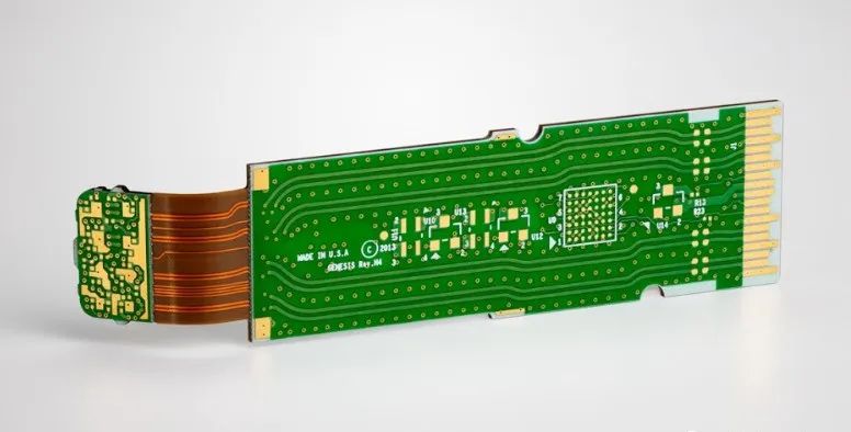
Whether engineers or PCB manufacturers, they inevitably encounter PCB failures. The occurrence of these failures may lead to delays in product delivery, damage to the manufacturer’s reputation, and increased time and monetary costs. (Most importantly, it costs money.)
Today, we mainly discuss PCB failure modes and solutions. (It is recommended to save for later viewing, as images and text may not match, please ignore this.)
Here are 15 PCB failure modes:
-
1. PCB Cracking or Warping
-
2. Assembled PCB Components Have Obvious Polarity
-
3. PCB Solder Joint Fracture
-
4. PCB Corrosion
-
5. Electronic Components Burned Out or Damaged (Short Circuit)
-
6. Incorrect Copper Weight
-
7. Electronic Component Position Shift
-
8. Expired Warranty for Electronic Components
-
9. Dehumidification Caused by Melted Solder
-
10. Issues During PCB Soldering Process
-
11. Physical Issues with PCB Materials
-
12. Chemical Fluid Leakage in Electronic Components
-
13. PCB Design Failure
-
14. Poor Quality Electronic Components
-
15. PCB Placement Environment
1. PCB Cracking or Warping
Cause: Due to high mechanical or physical stress, printed circuit board assemblies (PCBA) may crack or warp. For example, if a rigid PCBA is subjected to repeated vibration or thermal shock, it may fail. Additionally, if the bending strength you apply exceeds its capacity, even a flexible PCBA may crack.
Prevention Method: Before using the PCB during assembly, pre-bake the PCB and store it in a humidity-controlled cabinet to remove any moisture from the bare PCB, avoiding impacts in the later stages of assembly.
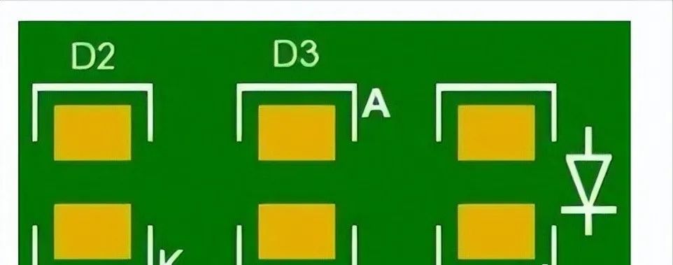
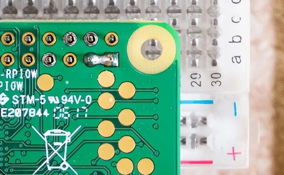
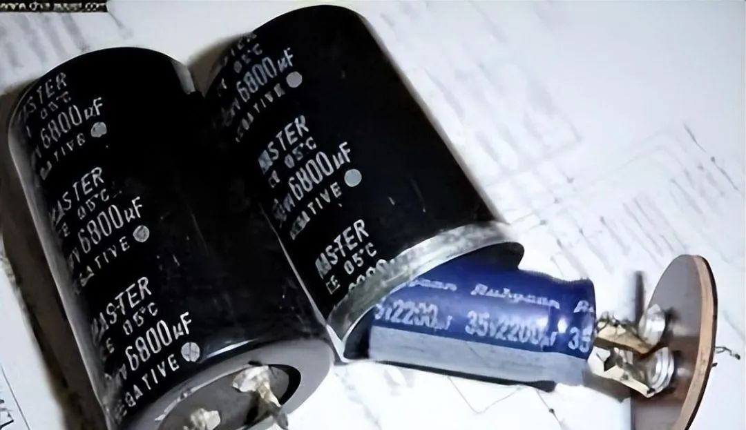
2. Assembled PCB Components Have Obvious Polarity
Cause: When designing the PCB layout, if the polarity of the components on the printed circuit board assembly is not obvious, it may lead to polarity reversal issues. For example, if the battery polarity is reversed, it may damage the battery and electrical components. The printed circuit board assembly may also fail and may cause electric shock.
PCB Components Have Obvious Polarity
Prevention Method: You can use diodes or Schottky diodes to mitigate the effects of reverse polarity. If you connect a diode in series with the battery, the circuit will shut off in the event of reverse polarity, preventing any significant damage to the printed circuit board assembly.
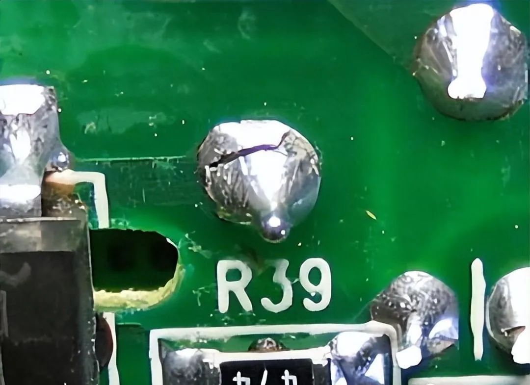
3. PCB Solder Joint Fracture
Cause: The difference in thermal coefficients between the PCB and electronic components may lead to solder joint fractures. If the printed circuit board assembly is subjected to repeated high or low temperatures, it may fail. Another reason may be manual soldering, which makes the solder more susceptible to thermal stress.
PCB Solder Joint Fracture
Prevention Method: It is much better if specialized automatic machines are used to solder electronic components. Please ensure that a visual inspection has been conducted before sending the PCB to the assembly process.
4. PCB Corrosion
Cause: Due to the use of flux during the PCB assembly process, some residues may lead to corrosion of the printed circuit board assembly. Flux is essential for ensuring the safe connection of electrical components. However, once in contact, it can also cause corrosion.
White Residue Causing PCB Defects
Prevention Method: Flux consists of organic acids, such as citric acid or adipic acid. PCB assemblers should ensure the removal of any excess flux from the PCB surface. This will prevent flux from damaging the metal contacts. If the PCB assembler uses a reflow oven, they should remember to wash off any excess flux.
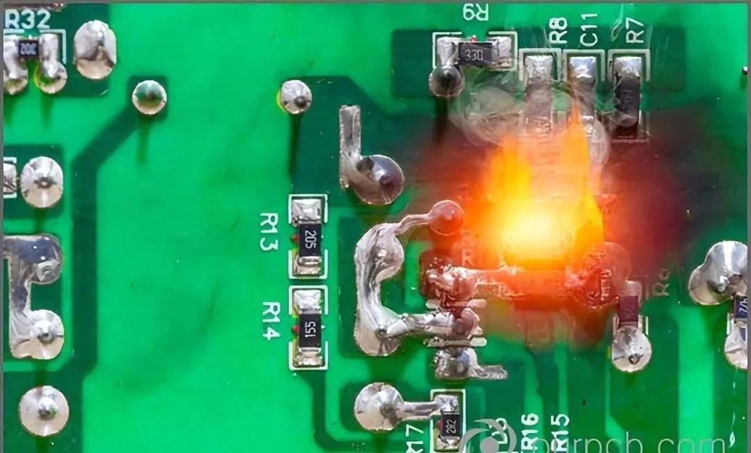
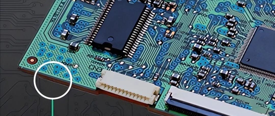
5. Electronic Components Burned Out or Damaged (Short Circuit)
Cause: During the PCB assembly process, short circuits may damage the PCB and electronic components. This may be due to undetected solder bridges, humidity, or unexpected events (such as high current spikes). Short circuits can cause sudden and catastrophic damage to components and may also lead to fires and damage to electrical equipment.
PCB Burned Out Due to Short Circuit
Prevention Method: Conduct visual inspections to check for short circuits on the PCB surface. For inner layers, electrical testing is most suitable for printed circuit board assembly, which primarily checks for shorts or opens. Additionally, you can compare the readings obtained with those from probe testing.
Furthermore, when designing the PCB layout, PCB assemblers must accurately align each layer. This way, they will be able to work in unison and avoid any short circuits. You can also reduce the thickness of the PCB template to minimize solder paste deposition.
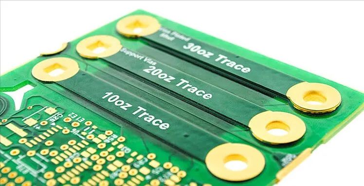
6. Incorrect Copper Weight
Cause: For good current flow in printed circuit board assemblies, the correct copper foil weight is necessary. If the copper weight is too thin or too thick, it can lead to failures in your printed circuit board assemblies, which is mainly due to improper sizing and trace width selection during PCB layout design.
Multiple Copper Weights on the Same Layer Circuit
Prevention Method: PCB assemblers must follow the copper weight specifications required by PCB engineers. Copper cannot be too thick, as it will increase costs, nor too thin, as it may lead to PCB overheating.
7. Component Position Shift
Cause: In PCB assembly, components are placed by pick-and-place or other automated machines. If components shift or move during soldering due to melted solder, the PCB may fail. This is mainly because reliable solder joints will not form and may lead to opens.
Prevention Method: PCB assemblers should adhere to standard humidity and temperature requirements, and they may use more precise pick-and-place machines for accurate component placement. Additionally, if you also use more corrosive flux, it will enhance the solderability of the parts, which can keep electronic components in their original positions.
Incorrect Adjustment of Component Position
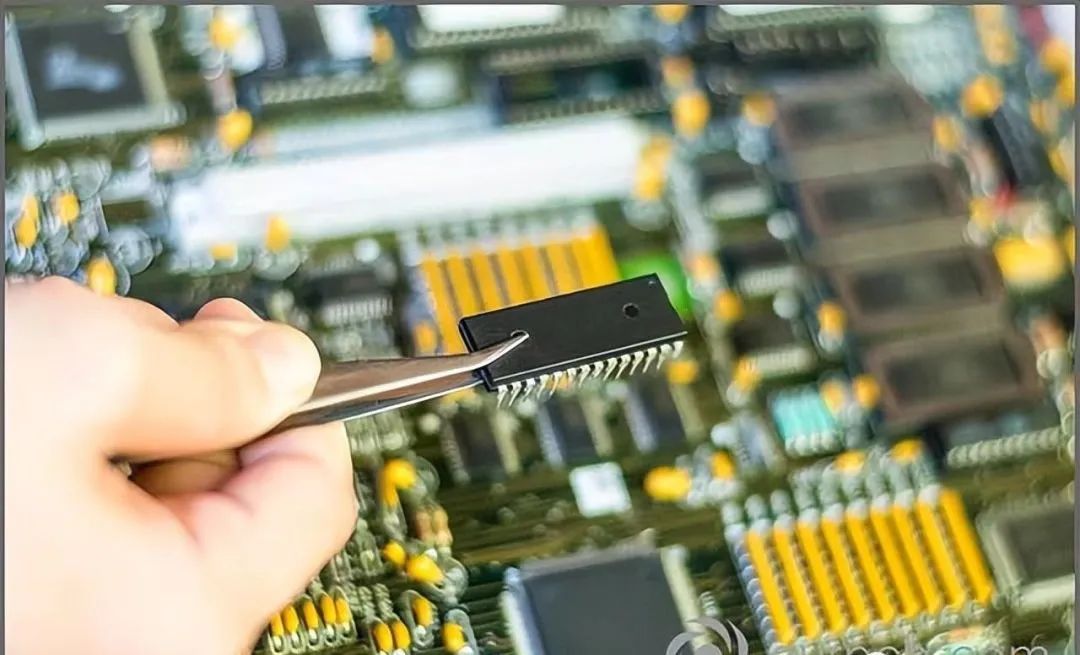
8. Expired Warranty for Electronic Components
Cause: If any individual component in the printed circuit board assembly fails, it may lead to the collapse of the entire PCB assembly, and parts may fail due to adverse selection. It would be helpful to ensure that these components do not have limited warranties. Additionally, if you choose low-quality components, it will reduce the lifespan of the parts and may even fail before the warranty period expires.
Various Electronic Components
Prevention Method: Components should be carefully selected or request your PCB factory to do so; parts should not be damaged or of low quality (electronic component backups). Additionally, you can directly add backups of components.
9. PCB Thermal or Moisture Stress
Cause: Different materials have different expansion rates; therefore, when constant thermal stress is applied, it can damage solder joints and components. If the wrong copper weight is used or there are plating issues, the stress from thermal factors will increase. Even during manufacturing, the temperature of the room where the PCB is assembled will affect its performance.
Assembling Circuit Boards
Prevention Method: PCB assemblers must conduct careful inspections of the circuit boards, prepare adequately, and perform necessary cleaning. Pencil erasers can eliminate any minor corrosion or rust. You can identify matte copper pads by their deep brown color. Solder will not adhere to surfaces affected by rust and must be cleaned before application, and excess should be removed with solder core.
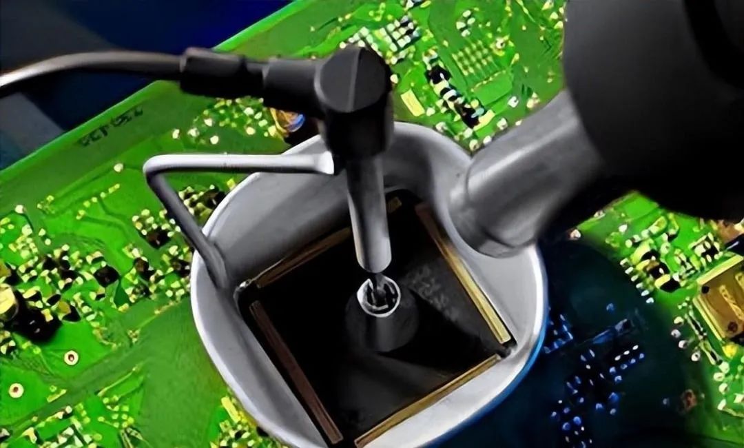
10. Issues During PCB Soldering Process
Solder is crucial for the operation of electronic circuits, hence requiring extra attention. The most common solder-related issues are flux contamination and poor processing conditions. Flux is a chemical cleaner used before and during soldering electronic components to the circuit board, some flux residues can absorb moisture that may conduct electricity, leading to short circuits. If the soldering process is not correctly set up and controlled, it may lead to open joints and contamination.
Issues During PCB Soldering Process
11. Physical Issues with PCB Materials
The materials used in PCBs often encounter issues that lead to board failure. During the manufacturing stage, if a layer of the PCB is misaligned, it can lead to shorts, opens, and crossed signal lines. If materials have psychological defects such as fractures, voids, and delaminations, they will severely impact PCB performance; if the materials used are not pure, failures may also occur.
Issues During PCB Soldering Process
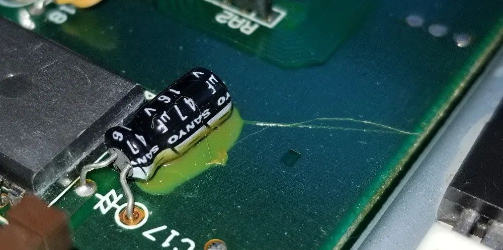
12. Chemical Fluid Leakage in Electronic Components
The presence of any chemical liquids leaking from components can severely damage the PCB and cause failures. Most chemicals are removed during manufacturing. However, trace elements may remain. Leakage may occur inside the packaging of components, leading to rapid aging of semiconductors or packaging. This chemical leakage can ultimately lead to short circuits or corrosion.
Chemical Fluid Leakage in Electronic Components
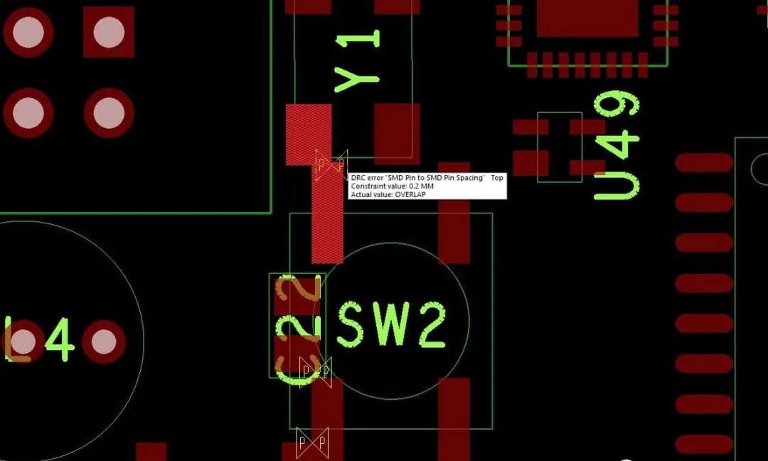
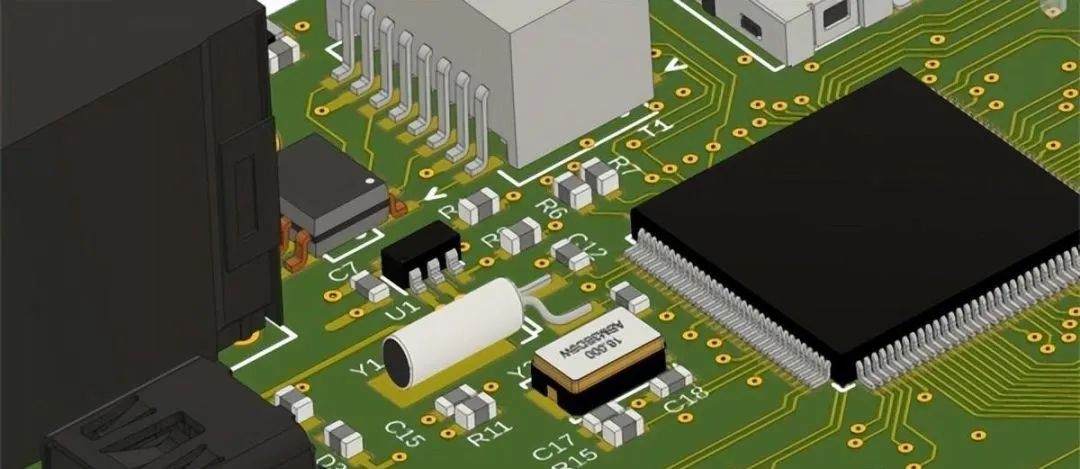
13. PCB Design Failure
One of the most common causes of PCB failures is incorrect component placement due to insufficient PCB space, power supply failures, or overheating. Space is critical, especially as circuit boards become more complex and need to meet stringent requirements. Here are just a few examples of potential errors during the design and manufacturing stages. Don’t forget that many such issues can be avoided by following correct PCB design rules.
-
-
-
-
Incorrect Component Placement
-
14. Poor Quality Electronic Components
Finding electronic components that meet circuit design specifications is not easy, whether it’s ensuring packaging or managing components, finding quality electronic components is crucial when considering PCB assembly and manufacturing.
Tightly placed traces and pathways, poorly soldered cold solder joints, poor connectivity between circuit boards, insufficient board thickness, and the use of counterfeit components are just some of the issues that may arise.
15. PCB Placement Environment
Exposure of PCBs to heat, dust, and moisture, accidental impacts (drops and falls), and power overload/surges can all be causes of circuit board failures. However, the most destructive cause of premature circuit board failure is electrostatic discharge (ESD) during the assembly phase. Electrostatic discharge (ESD) is the sudden flow of current caused by contact shorting or dielectric breakdown between two charged objects. Electrostatic buildup may be caused by triboelectric charging or electrostatic induction.

Source: Circuit One Point
Copyright Statement: The copyright of the above text and images belongs to the original author. The “Meizhou Printed Circuit Industry Association” shares this as a reprint. If there are any copyright issues, please contact us for deletion.