Quick PCB is dedicated to becoming the most influential training base for PCB design talent.
Therefore,
PCB Girl
decided

To launch a series of PCB design basic knowledge sharing on the Quick PCB Academy WeChat public account,
along with project case analysis,
to enable students to apply what they learn.

To understand the knowledge related to PCB design,
we need to start with the concept of “PCB”.
In this issue, PCB Girl will first help students understand
what is “PCB”?

PCB: Printed Circuit Board, also known as a printed circuit board, is the carrier of electronic components in electronic products and provides the connection for electronic components. Traditional circuit boards use the method of printing and etching resistors to create circuit lines and layouts, hence the name printed circuit board or printed wiring board.
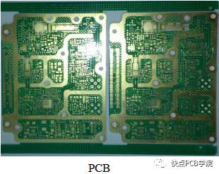
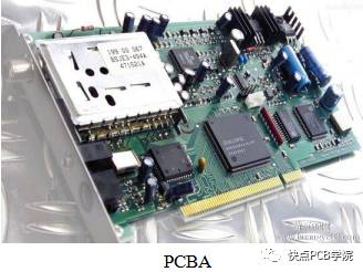
To understand the concept of printed circuit boards, it is first necessary to distinguish between PCB and PCBA.
The circuit boards we usually see are those that have components soldered onto the PCB, which is called PCBA (PCB Assembly). PCB refers to the “bare board” or “clean board”, meaning that PCB is the circuit board before components are soldered on. Only after the processing and assembly of PCB with electronic components does it form the circuit board used in electronic products.

In 1925, Charles Ducas from the United States printed circuit patterns on an insulated substrate and established connections through electroplating. This marks the beginning of modern PCB technology.
In 1947, epoxy resin began to be used for manufacturing substrates.
In 1953, Motorola developed a double-sided board using the electroplated through-hole method, which was later applied to multilayer circuit boards.
In 1960, V. Dahlgreen created flexible printed circuit boards by adhering metal foil with printed circuits to plastic.
In 1961, Hazeltine Corporation in the United States referenced the electroplated through-hole method to produce multilayer boards.
In 1995, Panasonic developed the ALIVH multilayer printed circuit board.
In 1996, Toshiba developed the B2IT multilayer printed circuit board.
By the end of the 20th century, new technologies such as Rigid-Flex, embedded resistors, embedded capacitors, and metal substrates emerged, making PCB not only a carrier for interconnection but also an extremely important component in all electronic products, playing a crucial role in today’s electronic products.

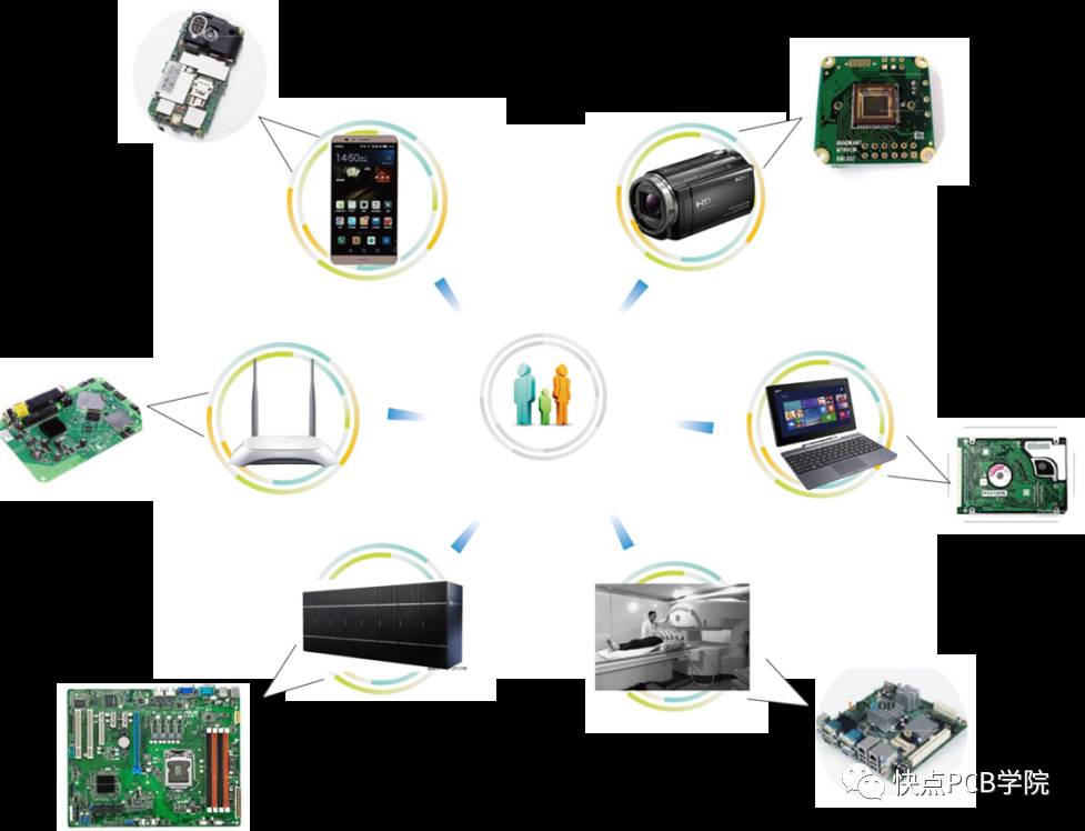
PCB is closely related to people’s daily lives. From personal devices like mobile phones, digital cameras, and laptops, to household devices like wireless routers and desktop computers, and larger equipment like MRI machines used in hospitals and wireless base stations used by telecom operators, PCB is required in all these products.
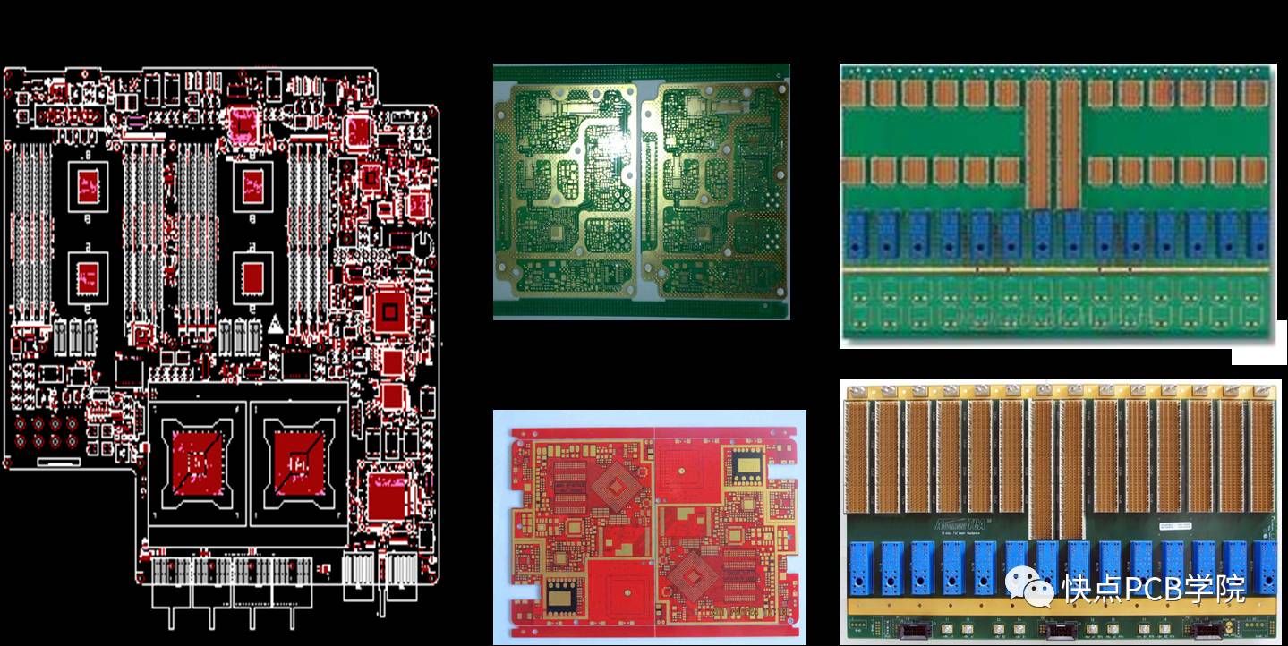
Examples of Different Types of PCB

PCB design, also known as PCB Layout, has evolved along with the continuous development of electronic products and can be divided into three main stages.
In the first stage, the signal rates of electronic products were low, and there were no challenges related to signal integrity. The focus of PCB design in this stage was to solve the “connectivity” problem, that is, to place components on the drawing according to circuit principles and connect the lines through wiring design without considering too many factors.
In the second stage, as the signal rates of electronic products increased, signal integrity issues became prominent. This stage introduced the concept of “rule-driven design”; this means that before the formal PCB design, design requirements from various aspects are transformed into specific design rules that can be implemented and operated in PCB design through simulation analysis or requirement decomposition and defined in the design drawings using professional software. This allows for real-time monitoring of the fulfillment of various requirements while the PCB design is being implemented, ensuring the functionality and performance of the circuit board.
In the third stage, with product miniaturization, new materials, new processes, and high-density designs, PCB design requires more familiarity with the characteristics and properties of materials and processes, considering the special requirements of high-density product design, such as HDI board design and chip packaging substrate design.
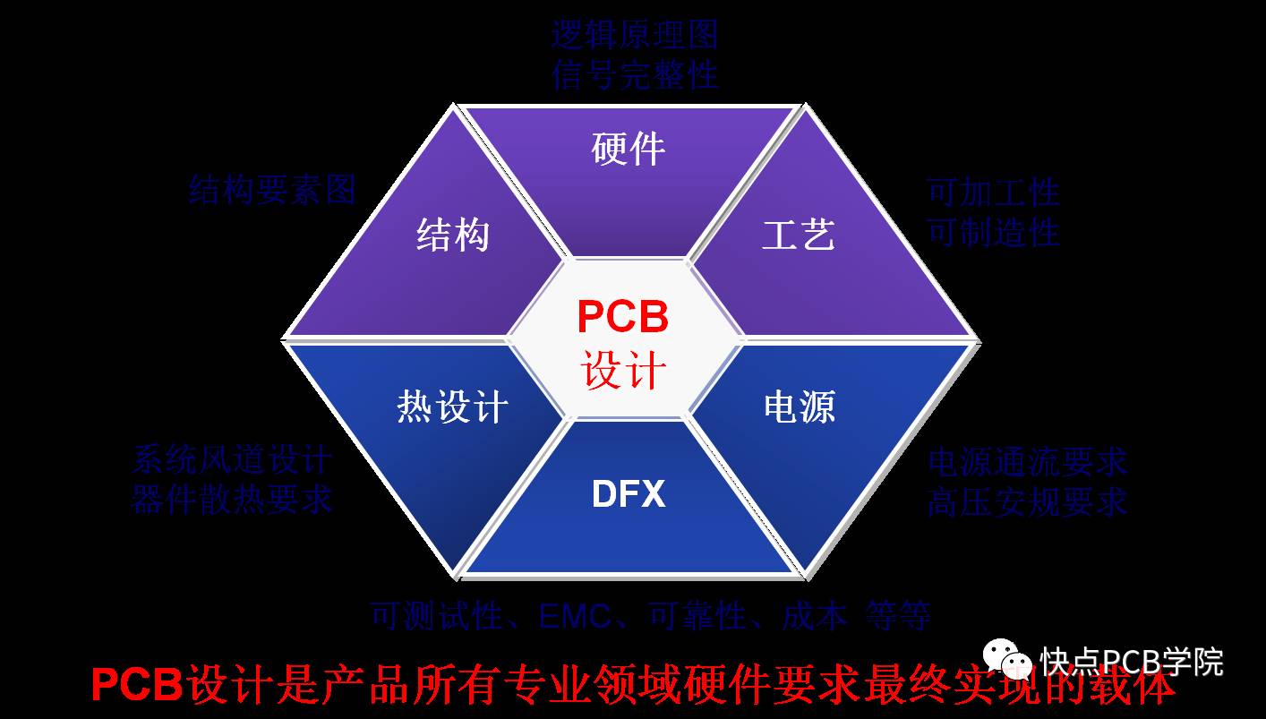
Design requirements in related fields of PCB
PCB design increasingly relies on powerful EDA design software tools and platforms. Designers not only need basic design concepts and methods but also need to understand the new requirements for PCB design brought about by the development of new products and technologies.
As mentioned above,
PCB design needs to rely on powerful EDA design software tools.
In the next issue, PCB Girl will introduce to students
the functions and methods of various mainstream PCB design software
and the installation steps for the most widely used
Cadence Allegro software,
which will be thorough and detailed.
Please stay tuned to
the 【Quick PCB Academy】 public account.
The only high-speed PCB design examination certification/training and employment platform certified jointly by the Ministry of Human Resources and Social Security and the China Employment Association.
Authoritative certification, a wealth of case studies, high-paying offers, and a clear path for advancement. Just visit Quick PCB (www.eqpcb.com)!
The most influential high-speed PCB design B2C platform in China.
Over 1,000 companies can post needs with one click, and over 5,000 layout engineers can easily take orders.
0755-84719081
Follow the Quick PCB career planning platform for the latest industry information and technical insights!