Wherever there is electricity, there are printed circuit boards (PCBs).
This course will share the basic knowledge of electroplating in PCB/HDI manufacturing. Due to the numerous knowledge points, it will be introduced in batches, and this is the first article.
Course Objectives
Understand what HDI is, the fields of application for HDI products, and the basic processes of HDI boards.
Familiarize with the electroplating process of HDI boards, key control points in the process, and product quality requirements.
Be aware of the impact of key control point failures on products.
1. Overview of HDI
1.1. Abbreviation of HDI Board:
HDI board stands for High Density Interconnect. It is a relatively new technology developed in the PCB industry at the end of the 20th century. Traditional PCB drilling is limited by the drill bit, and when the hole diameter reaches 0.15mm, the cost becomes very high, making further improvements difficult. HDI boards do not rely on traditional mechanical drilling but instead use laser drilling technology (hence sometimes referred to as laser boards). The hole diameter for HDI boards is generally 3-6 mil (0.076-0.152mm), the line width is typically 2-4 mil (0.05-0.10mm), and the pad size can be significantly reduced, allowing for more line distribution per unit area, leading to high-density interconnection. The emergence of HDI technology has adapted to and promoted the development of the PCB industry, enabling denser arrangements of BGA, QFP, and other components on HDI boards.
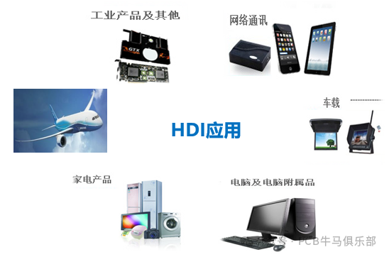
1.2. Applications of HDI
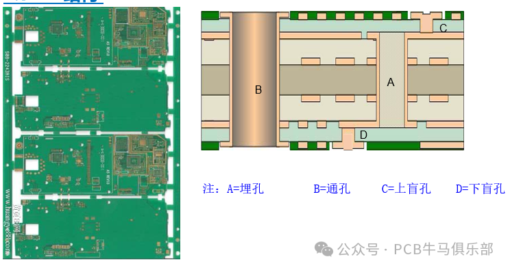
1.3 HDI Structure (taking a first-order buried blind hole as an example)
1.4 Overview of HDI Process Flow:
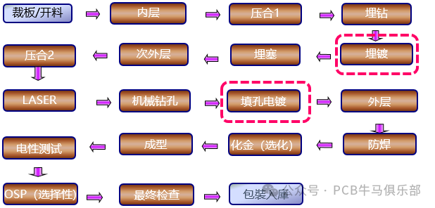
Note: Since HDI is a cyclic process, each additional step of lamination, laser, electroplating, and routing will add one more layer to the HDI board.
2. Purpose of HDI Electroplating Process
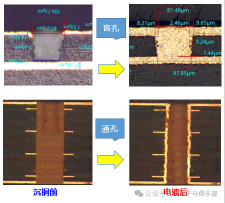
After drilling (through holes) or laser (blind holes) on HDI circuit boards, the interlayer conductive layers are insulated and cannot achieve electrical conduction. To enable electrical interconnection between the insulated interlayer conductive layers, the walls of the drilled (through holes) or laser (blind holes) on the HDI board need to undergo copper deposition to form a thin conductive layer inside the holes, followed by electroplating to thicken the copper, thus metallizing the originally non-conductive through holes/blind holes to meet the interconnection requirements between different layers of the HDI board.
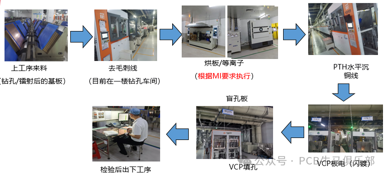
3. HDI Electroplating Process Flow (Blind Hole Board)
3. HDI Electroplating Process Flow (Pure Through Hole Board)
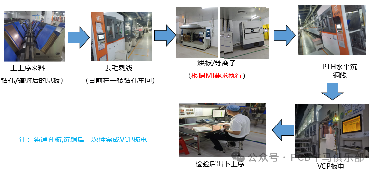
4. Functions/Key Controls/Quality Inspection of HDI Electroplating Subprocess
1. Version Verification: Check if the physical board, work order, and system (data) are consistent;
2. LOT Number Verification: Check if the work order number (lot) matches the MI data;
3. Process Flow Verification: Check for any deviations in the process;
4. Previous process: Check if there are signatures or stamps in place;
5. Verify if the previous process has undergone IPQC inspection and if there is an ACC stamp or signature;
4.1.2 Incoming Material – Quality Inspection:
4.2.1 Deburring – Subprocess Function:
Deburring Function
Utilizing the high-speed rotation of the brushing wheel to create friction on the board surface, removing fingerprints, oxidation, drill burrs, and other defects from the board surface;
Using high-pressure water washing to remove PP debris from inside the holes, preventing blockage before electroplating and ensuring no hole breakage after plating;
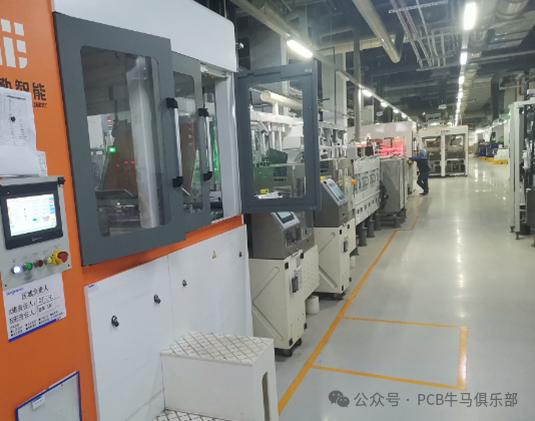 The following is the general process of the deburring line
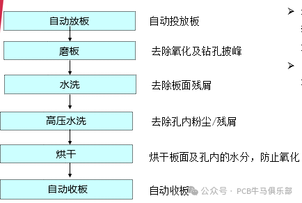
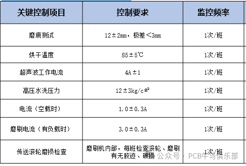
4.2.2 Deburring – Key Control Points:
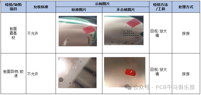
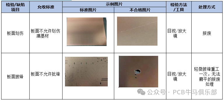
4.2.3 Deburring – Quality Inspection:
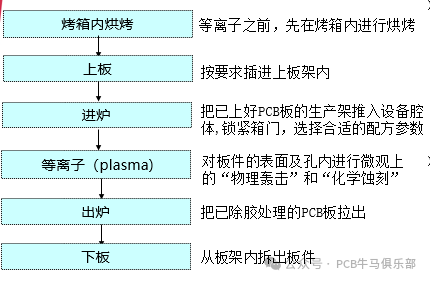
4.3.1 Plasma – Subprocess Function:
Plasma Function
In a sealed chamber under vacuum and at a certain temperature, specific gases such as nitrogen, oxygen, tetrafluoromethane, hydrogen, or argon are introduced. Under the influence of radio frequency electrodes, high-speed plasma is formed to perform microscopic “physical bombardment” and “chemical etching” on the surface and inside the holes of the board, achieving the effect of “removing glue” or “activating” the substrate position inside the holes.
Before plasma treatment, the board generally needs to be baked to remove moisture and release stress, preventing board breakage in subsequent processes or at the client site.
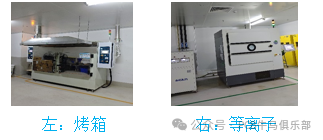
The following is the basic process of the plasma step:
To be continued!!! This is Part (1), and there will be sequels, so stay tuned!
Special Note: The above discussion is for reference only and serves as a starting point for further exploration! Each factory’s chemicals, processes, equipment, product structures, etc., have various differences, and one must not rigidly apply these experiences. All effective improvement measures come from experimental data! As a professional quality of engineering technicians, one must “speak with data.”
This public account will continue to update information related to PCB manufacturing and cutting-edge technologies.
Thank you, not only for being so good-looking and handsome but also for using your golden fingers to follow, collect, like, share, and comment!!!
Original content is not easy; if you want to reprint, please private message the author, obtain consent, and indicate the source before reprinting. Thank you for your cooperation!