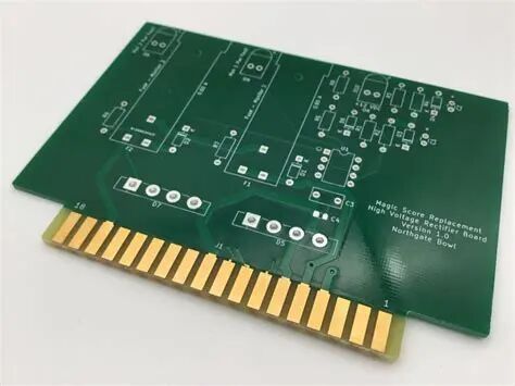
Printed Circuit Board
PCB Design
Printed Circuit Board (PCB) design is one of the core skills in electronic engineering, essential for both simple electronic projects and complex industrial products.
1.PCB Design Basic Process
1. Schematic Design
Use EDA tools (such as Altium Designer, KiCad, Eagle) to draw the circuit schematic and define the connections between components.
Ensure that the schematic symbols match the component footprints.
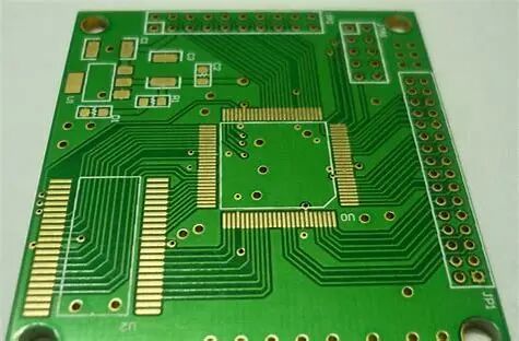
2. Component Layout
Divide the circuit into modules based on functionality (power supply, signal processing, interfaces, etc.).
Keep high-frequency/sensitive signal paths as short as possible, and place heat-generating components away from sensitive devices.
Consider installation dimensions, heat dissipation, and mechanical structure limitations.
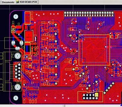
3. Routing
Signal Priority: Route high-speed signals (such as clock lines) first, avoiding long parallel runs.
Power and Ground: Widen power/ground traces, and use copper pour to reduce impedance.
Differential Pairs/Impedance Control: High-speed differential signals require equal-length routing, and specific impedance requirements necessitate calculations for trace width and stack-up structure.
4. Design Rule Check (DRC)
Check for line spacing, via sizes, shorts/open circuits to ensure compliance with production specifications.
5. Output Production Files
Generate Gerber files (photoplot files for each layer), drill files (NC Drill), and BOM (Bill of Materials).
2.Core Concepts of PCB Design
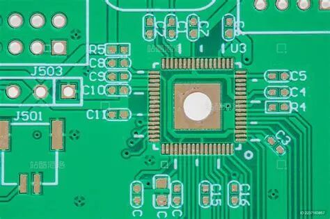
1. Layers
Single-sided, double-sided, multi-layer boards (4 layers, 6 layers and above), multi-layer boards are commonly used in high-frequency designs to reduce interference.
Typical layer classifications: signal layers, power layers, ground layers, silkscreen layers, solder mask layers.
2. Vias
Through-hole, blind vias, buried vias, used to connect different layers.
3. Trace Width and Current
Trace width must be designed according to the current size (for example, a current of 1A corresponds to a trace width of about 0.3mm, refer to IPC standards).
4. Clearance
High voltage or high-frequency circuits require increased spacing to avoid breakdown or crosstalk.
3. Common Design Tools
1. Beginner-Friendly
KiCad: Open-source and free, suitable for learning and small projects.
EasyEDA: An online tool that supports direct production orders.
2. Professional Level
Altium Designer: Comprehensive features, the first choice for industrial-grade design.
Cadence Allegro: Commonly used for high-speed/complex PCB designs.
PADS: Commonly used by small to medium enterprises, cost-effective.
4. Key Design Principles
1. Electromagnetic Compatibility (EMC)
Avoid right-angle traces (use 45° or arcs) to reduce antenna effects.
Maintain a complete ground plane beneath high-frequency signals to suppress interference.
2. Thermal Management
Place heat-generating components (such as power MOSFETs) near the board edge or add heat dissipation holes/heatsinks.
Avoid placing heat-sensitive components (such as electrolytic capacitors) near heat sources.
3. Design for Manufacturability (DFM)
Pad sizes must meet component specifications (to avoid cold solder joints).
Leave test points (Test Point) and debugging interfaces.

5. Common Mistakes and Precautions
Mistake: Ignoring ground loop design, leading to noise interference.
Solution: Use star grounding or single-point grounding to ensure a complete ground plane.
Mistake: Insufficient power filtering.
Solution: Add decoupling capacitors (such as 0.1μF) near the power entry and chip power pins.
Mistake: Silkscreen covering pads, affecting soldering.
Solution: Adjust silkscreen positions, focusing on DRC checks.
PCB design is a combination of theory and experience, requiring knowledge of tool operation, circuit principles, and production processes. It is recommended to start with simple projects and gradually accumulate design experience while paying attention to industry standards (such as IPC7351) and the latest technology trends (such as high-speed signals and flexible PCBs).
END