
 ▲ Click the public account card above to follow for more information ▲
A packaging library mainly consists of two parts: pads and graphics. The position and size of the pads determine the soldering conditions, while the graphics serve to visually represent the component status, assisting in design and guiding component assembly.
We have discussed surface mount pads; in this chapter, we will talk about through-hole pads.
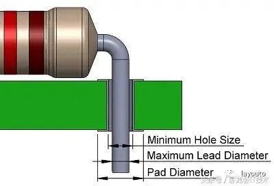
Through-hole pads, also known as plated through-hole pads, are actually more accurately referred to as hole pads (which sounds less appealing). They provide connection points for the leads of components and the electrical connections between the layers of the printed circuit board (PCB). The following image illustrates the core factors in the design of a through-hole pad, where the component manufacturer will provide the maximum lead diameter.
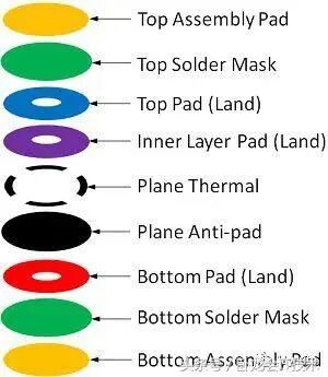
The following image is just aesthetically pleasing, included for fun.
Hole Diameter
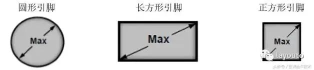
The common lead shapes are circular or rectangular. The main influencing factor for hole diameter design is the maximum length of the lead cross-section (represented by lead diameter here). The lead diameter is shown in the following image:
The calculation for hole diameter is based on the lead diameter, allowing space for the lead insertion and solder wicking to achieve better installation and soldering strength. Different levels of manufacturability correspond to different values, as shown in the table below. The hole diameter is obtained by directly adding this value to the lead diameter.
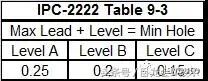
The Lecel A, B, C defined in IPC2221 1.6.3 can be referenced, with Level B being the commonly used grade.
Pad Diameter
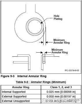
Component manufacturers usually provide recommended values for pin or hole sizes but do not provide pad sizes. All pad designs should aim for the widest possible annular ring, but designs often require more space to achieve higher density. Original content from today’s headlines: Wolonghui IT Technology. Therefore, we hope to meet the best performance with the minimum annular ring.
The main factors affecting pad design are hole diameter, minimum annular ring, and manufacturing tolerances. The calculation method is:
Minimum pad diameter = hole diameter + 2 * minimum annular ring + manufacturing tolerance
Minimum Annular Ring
Manufacturing Tolerance
IPC-2221B Table 9-1 Minimum manufacturing tolerances
Level A 0.4 mm
Level B 0.25 mm
Level C 0.2 mm
The above algorithm is for the minimum pad size. It is also common in the industry to use 1.5 times the hole diameter as the pad size, which has its reference basis. Of course, this value is also recommended as long as it meets the minimum pad requirement.
Hot Air Pads
The design of hot air pads is to insulate the conductor layer. Insulation is only necessary for large area conductors that need soldering (ground layers, power layers, thermal layers). Insulation provides thermal resistance during the soldering process to reduce soldering time and achieve better soldering results.
Strap Width
The width of each strap is typically determined by dividing 60% of the pad diameter by the required number of straps (we usually use 4 straps).
Width of 4 straps = 60% * minimum pad diameter / 4
Inner and Outer Diameter
The design of the inner diameter (ID) and outer diameter (OD) of hot air pads is related to the hole diameter. Different levels of manufacturability correspond to different values exceeding the hole diameter, as shown in the following image:
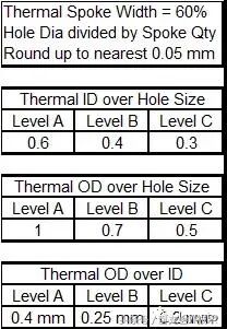
Here’s a question: shouldn’t 0.7 – 0.4 equal 0.3? Why does the image show 0.25?
Isolation Diameter
Hot air pads also involve a parameter called the isolation pad (Anti Pad). For standard through-hole pads, Anti Pad = OD. For non-metalized holes, it also involves the gap from the connection pad to the layer.
Isolation Diameter = Minimum Pad – 2 * Minimum Annular Ring + 2 * Gap from Connection Pad to Layer
Isolation Diameter = Hole Diameter + Manufacturing Tolerance + 2 * Gap from Connection Pad to Layer
It can be logically inferred that the results of the two algorithms above are the same.
IPC-2222A Table 9-1 Gap from Connection Pad to Layer
Level A 0.51 mm
Level B 0.25 mm
Level C 0.13 mm
Manufacturability Levels
Based on design characteristics, tolerances, measurements, assembly, finished product testing, and manufacturing process validation, manufacturability can be divided into three levels to reflect the increasing complexity in positioning, materials, processes, etc., while the production costs also increase accordingly.
Level A: General Design Manufacturability — Preferred
Level B: Intermediate Design Manufacturability — Commonly Used
Level C: High-Difficulty Design Manufacturability — Reduced
Manufacturability levels do not represent design requirements but indicate a method of assessing the difficulty between design and production assembly. When one characteristic uses a certain level, it does not require other characteristics to use the same level. The manufacturability level should be determined based on precision, performance indicators, conductive pattern density, equipment, installation, and testing requirements, while the selection should be based on meeting the minimum needs.
This article is edited and reprinted for the purpose of conveying more information and does not represent the website’s endorsement of its views or responsibility for its authenticity. Copyright belongs to the original author. If there are issues regarding the content, copyright, or other matters, please contact this public account within 30 days WeChat (kunyi346416), and we will delete the content promptly! ▼Click the link below to follow the recommended public account▼

 ●【Technical Article】This current detection circuit, you probably don’t know about it!●【Technical Article】Bluetooth: Why is it called “Bluetooth” and not “White Tooth”?●【Resource Collection】Collection | Comprehensive PCB Production Process●【Resource Material】104 PCB Design Tips Q&A | Worry-Free Board Design!●【Technical Resource】PADS, is this enough? Comprehensive list of non-mold commands●【Resource Sharing】Planning to enroll 200 students, free learning of high-speed PCB

If you find the content good, please give it a thumbs up!