Understanding Printed Circuit
Boards and Altium Designer
Printed Circuit Boards (PCB) are the core components of electronic devices, used to connect and support electronic components.Altium Designer is the industry-leading PCB design software, widely used in the field of electronic design.
1. Basic Knowledge of Printed Circuit Boards (PCB)
1. Structure of PCB
Substrate: Usually made of fiberglass (FR4), which has insulation and mechanical strength.
Copper Layer: Conductive layer, formed by etching to create circuit traces.
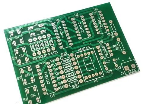
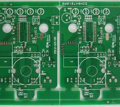
Solder Mask: A protective layer covering non-soldering areas, usually green.
Silkscreen: Used for labeling component identifiers, symbols, or text.
2. Types of PCB
Single-sided: Only one side has a copper layer, low cost, suitable for simple circuits.
Double-sided: Both sides have copper layers, connected by vias.
Multilayer: 4 layers or more, including internal power and signal layers, suitable for complex circuits.
3. Design Process
Schematic Design → PCB Layout → Routing → Design Rule Check (DRC) → Generate Manufacturing Files (Gerber).
2. Core Functions of Altium Designer
1. Schematic Design (Schematic Capture)
Library Management: Use built-in libraries or custom libraries (.SchLib).
Wiring Tools: Connect components using wires and net labels.
Electrical Rule Check (ERC): Ensures schematic logic is correct.
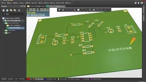
2. PCB Design
Board Shape Definition: Set board layers, dimensions, and shapes.
Component Layout: Manually or automatically arrange components to optimize signal integrity.
Routing:
Manual Routing: Control trace paths and widths.
Automatic Routing: Quickly complete using algorithms (requires later optimization).
Vias and Pads: Support through-hole, blind, and buried hole designs.

3. Advanced Features
3D View: Visualize the assembly relationship between the PCB and the enclosure.
Signal Integrity Analysis: Detect issues such as reflections and crosstalk in high-speed signals.
Design Reuse: Improve efficiency through snippets or modular design.
4. Output Files
Gerber Files: Used for PCB manufacturing (various layers of copper, solder mask, silkscreen, etc.).
BOM (Bill of Materials): A list of components for procurement and production use.
Drill Files (NC Drill): Guide PCB drilling machine operations.
3. Altium Designer Operation Tips
1. Shortcuts
T+P: Open preferences settings.
Ctrl+D: Toggle display/hide layers.
Tab: Modify properties when placing objects.
2. Design Rules
Set constraints for line width, spacing, via sizes, etc., to ensure compliance with manufacturing requirements.
Rule Priority: Local rules override global rules.
3. Multilayer Board Design
Use internal planes to allocate power and ground networks.
Split power planes to support multiple voltages.
4. Common Problem Solving
DRC Errors: Check for unconnected pins, spacing violations, etc.
Thermal Design: Increase copper area or add thermal vias.
By systematically learning PCB design theory and Altium Designer tool operations, one can gradually master the design capabilities from simple circuits to complex systems. It is recommended to start with practical projects, combining simulation and debugging to optimize designs.
END