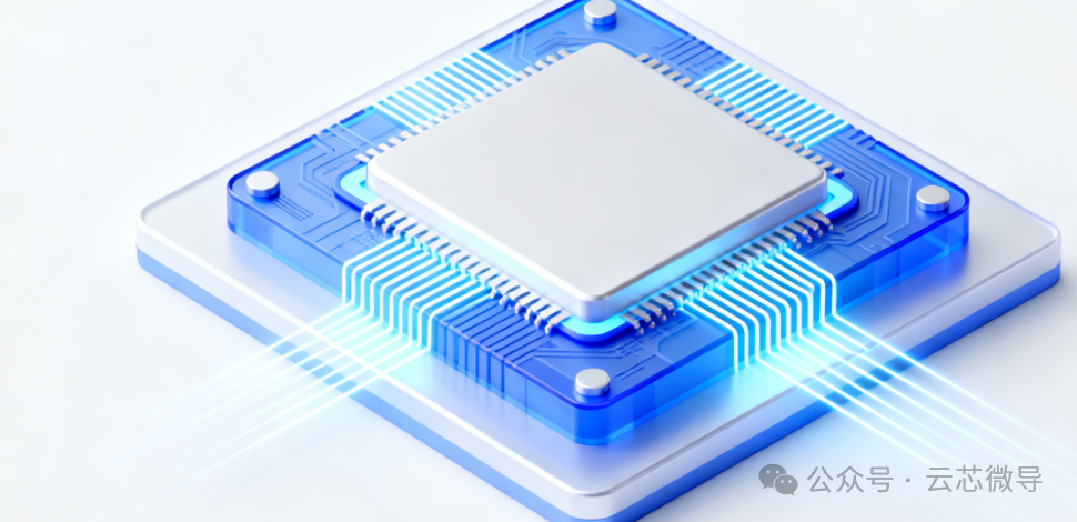
In the semiconductor industry, which pursues higher performance, smaller size, and lower power consumption, advanced packaging technology plays an increasingly important role. Among them, 2.5D packaging technology has become a significant milestone connecting traditional 2D packaging and true 3D packaging. The core of this technology lies in a key component known as the “interposer”.
1. What is an Interposer?
In simple terms, an interposer is an additional interconnection structure placed between the chip and the integrated circuit substrate.
Broadly speaking, any substrate or redistribution layer serves the function of being “between the chip and the PCB.” However, in the context of 2.5D packaging, the “interposer” specifically refers to those additional interconnection components that are added and placed on top of the conventional packaging substrate. It acts like a precise “overpass,” translating and connecting the high-density microcircuits on the chip to the relatively lower wiring density of the IC substrate.
Common materials for interposers include:
- Silicon interposer
- Glass interposer
- molded interposer
- RDL interposer
2. Main Functions of the Interposer
The primary function of the interposer is to achieve horizontal interconnection of multiple chips.
In 2.5D packaging, different chips (such as logic chips, memory chips, etc.) are placed side by side on the same interposer. The interposer is internally wired with extremely precise routing, connecting the input/output ports of these chips together. This allows for communication between chips over very short paths and with extremely high bandwidth, far surpassing the traditional method of installing them separately on a PCB.
3. Different Types of Interposer Interconnection Methods
The specific technology for achieving vertical interconnection with the interposer depends on its manufacturing material:
- Silicon interposer: This is the most mainstream technology. It uses TSV to achieve electrical connections in the vertical direction. TSVs are micro-holes etched on silicon wafers and filled with conductive materials (such as copper), making it the highest performance and most mature solution.
- Molded interposer: Uses TMV. Its principle is similar to TSV, but it forms through-holes on molded compound materials, usually at a lower cost.
- RDL interposer: This type of interposer does not have TSV or TMV; it directly utilizes its redistribution layer for horizontal interconnection. Vertical connections are achieved through bumps or solder points located above it.
- Glass interposer: Theoretically uses TGV. Glass, as an excellent insulator, has advantages in high-frequency applications, but this technology has not yet been widely adopted in the market.
4. A Key Process: Double-Sided Bonding
Regardless of the type of interposer used, a common and crucial process step is that the interposer needs to be bonded on both sides.
- The upper side connects to the chip through structures like micro-bumps.
- The lower side connects to the IC substrate through larger solder balls or bumps.
This double-sided bonding structure ensures a complete electrical path and mechanical support from the chip to the interposer and then to the substrate.
Conclusion
By introducing the innovative structure of the interposer, 2.5D packaging cleverly addresses the challenges of multi-chip, high-density interconnections. It not only establishes a “highway” for chip-to-chip communication in the horizontal direction but also completes the “three-dimensional traffic” in the vertical direction through technologies like TSV and TMV, significantly enhancing overall system performance. It is widely used in high-end processors, FPGAs, and artificial intelligence accelerator chips, making it one of the important engines driving modern computing technology forward.