
The leap from Transformer models to large language models seems unstoppable in the computing power revolution. However, you may not know that the real factor slowing down the evolution of AI chips is not the computing power itself, but an “old problem” we are already familiar with—memory.
In the latest research report from Stanford titled “GainSight: Application-Guided Profiling for Composing Heterogeneous On-Chip Memories in Next-Generation AI Accelerators,” a clear signal emerges:
Computing power is not the bottleneck; memory is the next battlefield.
In particular, on-chip memory is becoming a decisive variable in the architecture of next-generation AI accelerators.
SRAM Reaches Its Limits, the Memory Wall Approaches Quietly
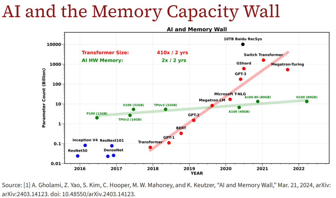
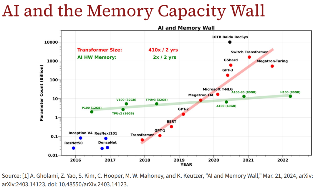
Looking back over the past decade, the number of parameters in AI models has grown exponentially. According to data cited in the paper, the size of Transformer modelsincreases 410 times every two years, while the memory capacity of AI hardware onlydoubles every two years.
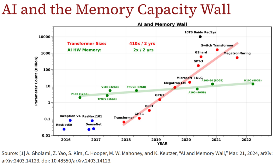
This creates a clear gap:models are growing rapidly, while memory is struggling to keep up.
The issue of the memory wall is not new. However, this time, the difference is that SRAM—our most commonly used on-chip cache—is facing two simultaneous limitations:
-
Density Bottleneck: The process of shrinking SRAM has plateaued; as we move below 32nm, the area savings become increasingly minimal;
-
Energy Efficiency Challenge: While it is fast, it consumes a lot of power and has a high cost per unit area, which is not friendly to the data structures of large AI models.
Not all data is worth storing in SRAM.
The report provides a key observation:the data in AI computation has an extremely uneven “lifecycle”. Some data only needs to be stored for a short time, while other data is rarely modified. Using SRAM to handle them uniformly is a waste.
GainSight: Uncovering the “Data Lifecycle”
The GainSight proposed by the Stanford team aims to solve this core problem.
It is not a chip, but an analytical toolchain. Its goal is clear:
To clarify which data in an AI workload (such as GPT or ResNet) is suitable for which type of storage structure.
This toolchain is divided into two parts:
1. Retargetable Hardware Backend
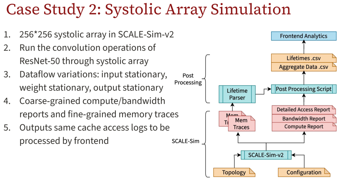
It collects every memory access record from GPUs or Systolic Arrays through simulators (such as Accel-Sim, SCALE-Sim), capturing fine-grained data: access frequency, lifecycle, read/write ratio, etc.
2. Analytical Frontend
It transforms the collected access logs into usable hardware metrics:
-
How long a piece of data has survived (Lifetime)
-
How much area each bit requires (Area Projection)
-
How much energy is consumed for read/write/refresh (Power Projection)
-
Whether it can be replaced with other structures like GCRAM, DRAM, or Flash
This is like adding a “telescope” to chip design—no longer guessing based on experience, but measuring with data.
“Not all cache misses are problems; it depends on who is stored behind them.”
GPU and Systolic Array: Two Sets of Data, One Trend
To validate the practicality of GainSight, the report team conducted two sets of experiments.
✅ Case 1: GPU Architecture
They simulated models like GPT-J, Stable Diffusion, and ResNet, finding:
-
In L1 cache, 40% of accesses involve short-lifecycle data;
-
After replacing with Gain Cell RAM, energy consumption decreased by up to 28%, especially suitable for frequently refreshed but short-lived data blocks.
✅ Case 2: Systolic Array Architecture
Using ResNet-50 for convolution tasks, they found:
-
79% of scratchpad accesses are short-term, which do not need to be stored for long;
-
Different data flows (input/weight/output stationary) significantly affect memory design choices.
This means:heterogeneous memory design is not optional, but a necessity.
In Conclusion: AI Chip Design Cannot Rely on “One Memory to Rule Them All”
This report makes it very clear:
-
SRAM is not omnipotent. It remains king, but not every position needs a king.
-
Short-lifecycle data is the majority. They are born quickly and disappear quickly, warranting a more “lightweight” storage method.
-
Hardware design should obey application characteristics in reverse. GainSight proves with facts: storage structures should be “managed by data classification,” rather than a one-size-fits-all approach.
·END·Follow “Semiconductor Industry Report”Stay updated with the latest industry newsThe original report has been included in the knowledge community, and you are welcome to join.

Disclaimer: All works marked “Source: XXX” in this public account are reprinted from other media, and the copyright belongs to the original author. This account is only for the purpose of conveying more information and does not serve commercial purposes, nor does it represent this account’s endorsement of its views or responsibility for its authenticity. For reprints, please contact the original source. (Some images are sourced from the internet; if there is any infringement, please contact for removal). For original reprints and commercial cooperation, please add WeChat:13671210275