The SPI bus is<span><span>a synchronous, bidirectional, full-duplex 4-wire serial interface bus</span></span>, originally proposed by Motorola. The SPI system consists of a “single master device + multiple slave devices.” It is important to note that as long as only one master device is active at any given time, multiple SPI master devices can exist in the system. It is commonly used for communication between EEPROMs, FLASH, real-time clocks, AD converters, digital signal processors, and digital signal decoders.
To achieve communication, SPI has a total of 4 signal lines, which are: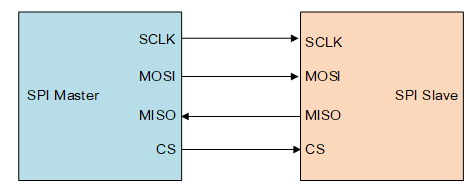 (1) Master Out Slave In (MOSI): This is the signal line for transmitting data from the master device to the slave device, also known as Slave Input (SI/SDI).(2) Master In Slave Out (MISO): This is the signal line for transmitting data from the slave device to the master device, also known as Slave Output (SO/SDO).(3) Serial Clock (SCLK): This is the signal line for transmitting the clock signal.(4) Slave Select (SS): This is the signal line used to select the slave device, which is active low.How to use SPI:
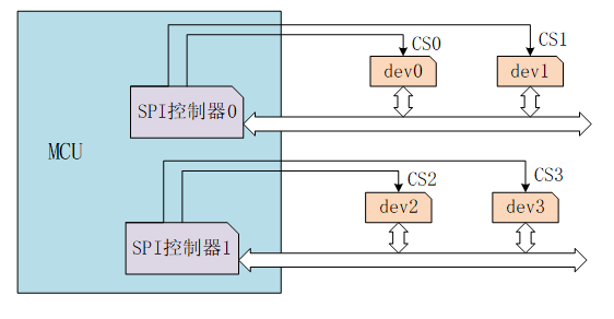 The chip shown in the figure has 2 SPI controllers, with each SPI controller corresponding to an SPI master device. Each SPI controller can connect to multiple SPI slave devices. The slave devices mounted on the same SPI controller share 3 signal pins: SCK, MISO, and MOSI, but each slave device’s CS pin is independent.The master device controls the CS pin to select the slave device, which is generally active low. At any given time, only one CS pin on an SPI master device can be active, allowing the slave device connected to that active CS pin to communicate with the master device.Therefore, the SPI communication method can use a “one master, multiple slaves” structure for communication. Each device connected to the bus has a unique address, the master device initiates data transmission and generates the clock signal, and only one master device is allowed at the same time.The clock for the slave device is provided by the master device through SCLK, while MOSI and MISO complete data transmission based on this pulse. The working timing mode of SPI is determined by the phase relationship between CPOL (Clock Polarity) and CPHA (Clock Phase). CPOL indicates the initial level state of the clock signal, where CPOL = 0 means the initial state of the clock signal is low, and CPOL = 1 means the initial level of the clock signal is high. CPHA indicates at which clock edge data is sampled; CPHA = 0 means data is sampled on the first clock transition edge, while CPHA = 1 means data is sampled on the second clock transition edge.Based on the different combinations of CPOL and CPHA, there are a total of 4 working timing modes: CPOL=0, CPHA=0; CPOL=0, CPHA=1; CPOL=1, CPHA=0; CPOL=1, CPHA=1.