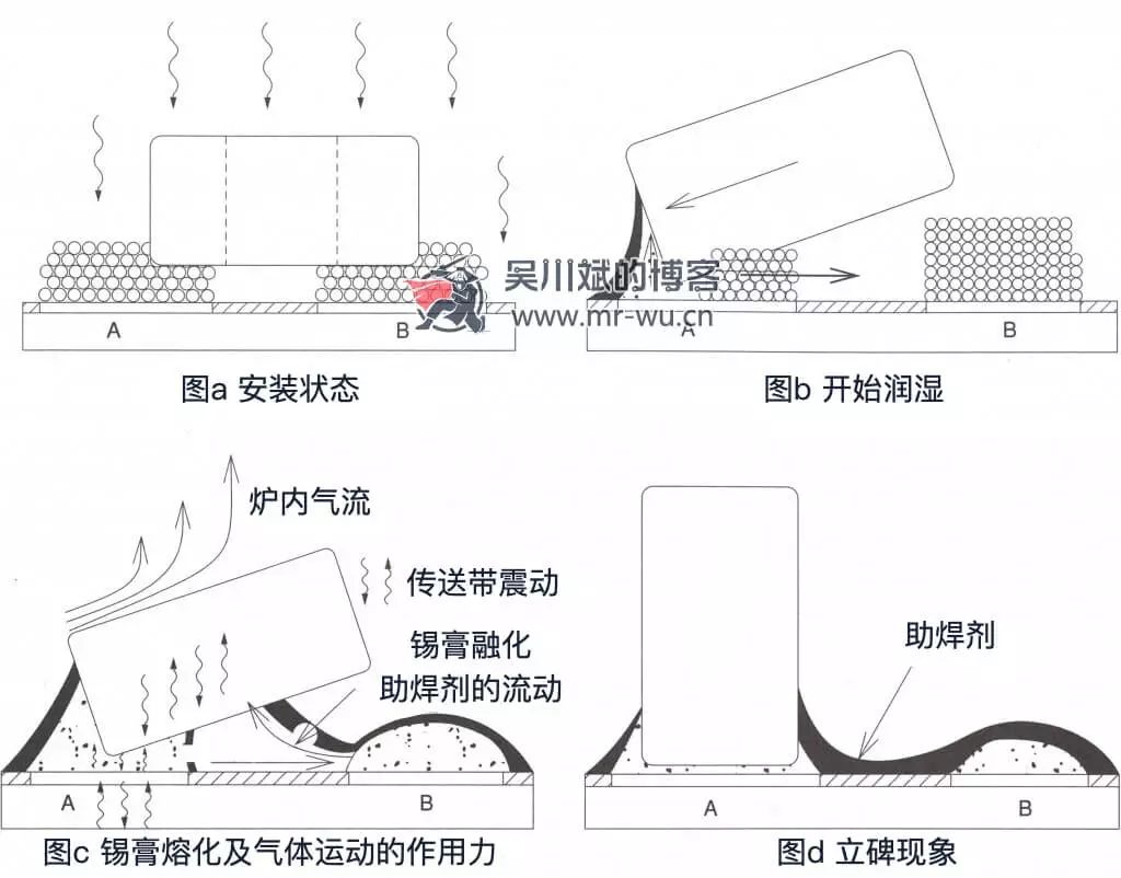
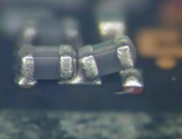
Tombstone defects on PCBs, also known as the Manhattan Bridge or bridge effect, are a type of assembly defect for surface-mounted (passive) components. This defect occurs due to inconsistent melting times of solder paste at both ends of the component, leading to uneven stress on the component. Given that these components are relatively light, they can tilt under stress, which is visually referred to as a tombstone.
Perhaps a pure text description is hard to understand, so I, Old Wu, am sharing a video of the SMT tombstone phenomenon for your reference.
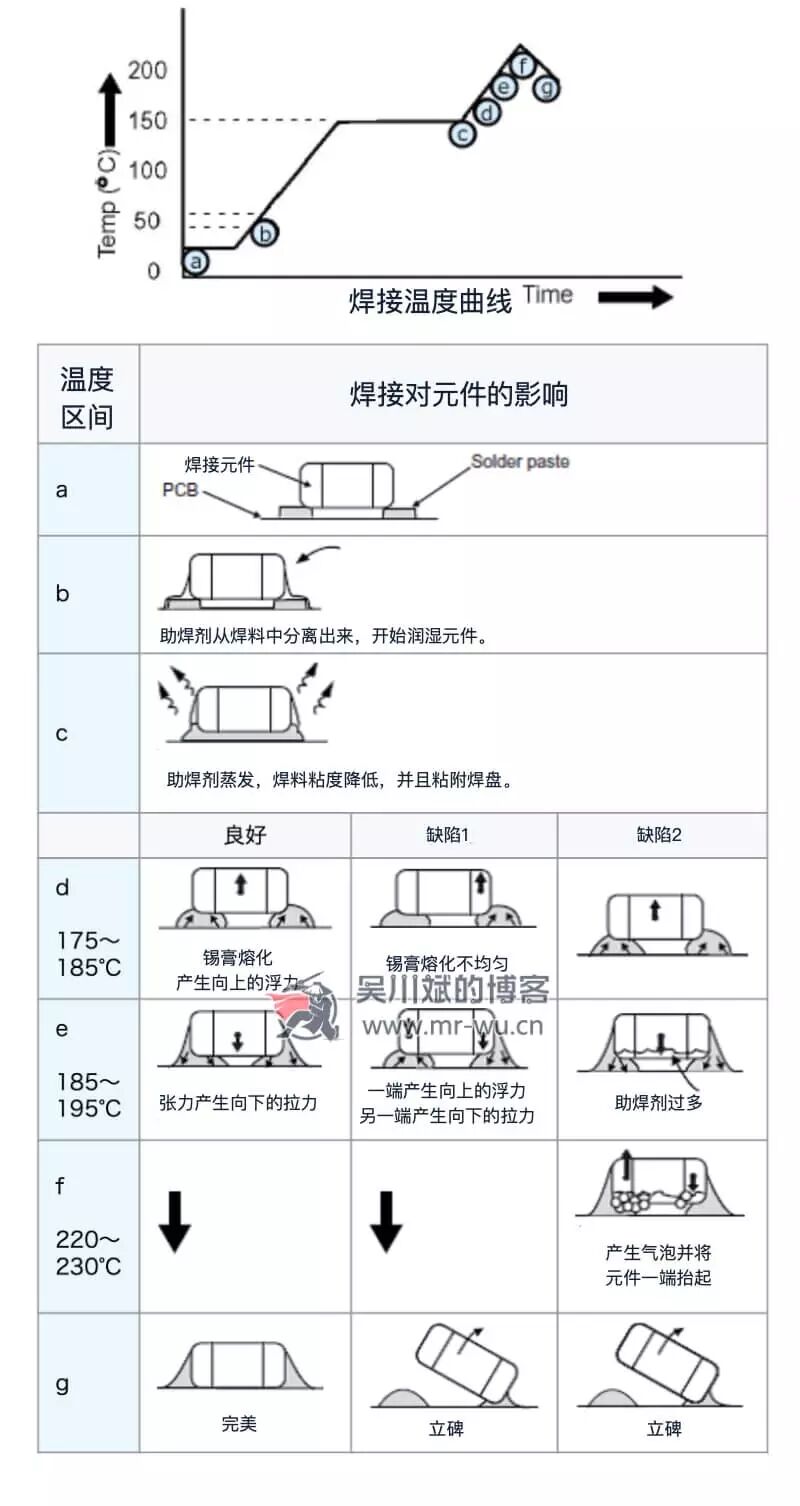
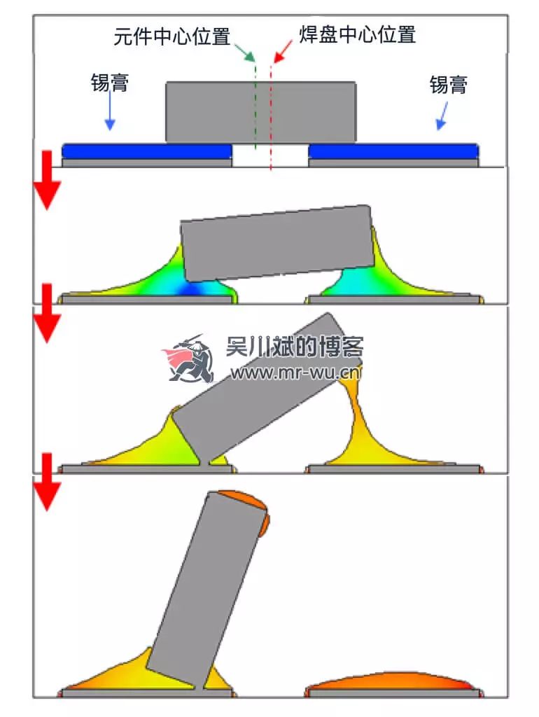
Before reflow or before the solder paste melts, due to the gel components in the solder paste, the component is held in place on the PCB pads by the adhesive force (f) of the solder paste and its own weight (G). When the PCB starts and stops on the conveyor, the components do not move.
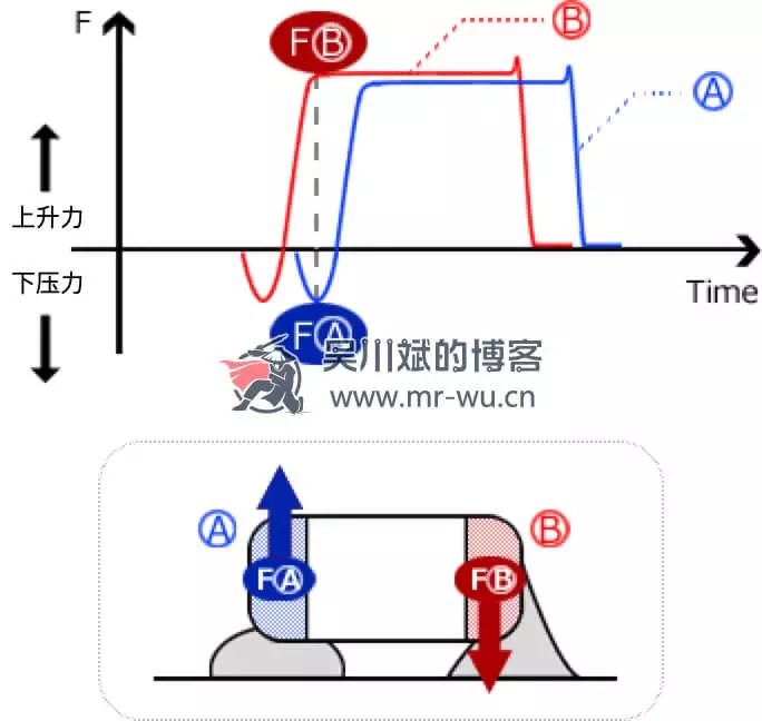
During the reflow stage, once the solder paste melts, the adhesive force (f) of the solder paste disappears. Before wetting begins, due to the surface tension of the liquid, the component is actually suspended on the surface of the molten solder, experiencing an upward buoyant force F’.
If the solder at the two pads of the component does not wet both soldering terminals simultaneously, or if there is a significant difference in the wetting rates at both ends, tombstone or displacement phenomena may occur.
In fact, tombstone defects mostly occur with surface-mounted capacitors or inductors, while resistors rarely experience this issue. This can be seen from the structural shape of the components; surface-mounted capacitors or inductors typically have square ends and a larger height, while resistors are generally smaller and rectangular. During the wetting process, the wetting lever arm L1 for square capacitors or inductors is certainly greater than that of resistors of the same size. Assuming the wetting forces are the same, a larger lever arm results in a greater torque, making the effect more pronounced. Therefore, the probability of tombstone defects occurring with resistors is relatively low.
How to Avoid Tombstone Failures Caused by SMT?
The key is to avoid uneven stress on the component during the soldering process.
If the solderability of the coating on the two solder terminals of the component is poor, and there is a difference in solderability between the two terminals, resulting in different wetting forces, this can lead to poor wetting, displacement, or tombstone issues.
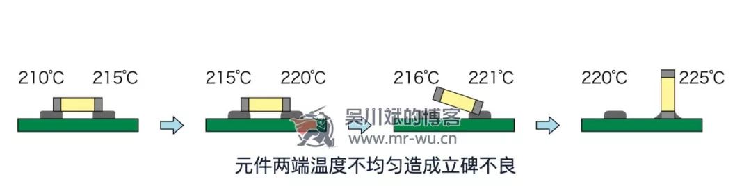
The reflow soldering furnace may have uneven temperatures, causing inconsistent temperatures at both ends of the chip. This temperature difference can lead to varying degrees of solder paste melting, resulting in stress differences that cause tombstone defects.
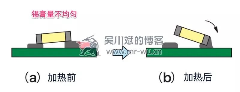
Significant differences in the volume of solder paste deposited on the two pads can lead to different amounts of heat required for melting the solder paste, resulting in differences in wetting and potentially causing displacement or tombstone issues.
If the solder paste printing is misaligned, and the solder paste is not fully deposited on the pads, this may prevent the component terminals from effectively contacting the solder paste, leading to either no contact or minimal contact, which can very likely result in tombstone or displacement issues.
Insufficient mounting accuracy can also lead to tombstone defects, which can be understood similarly to the misalignment of solder paste printing. If the solder paste cannot fully contact both terminals of the component, it can lead to differences in wetting, resulting in tombstone or displacement issues.
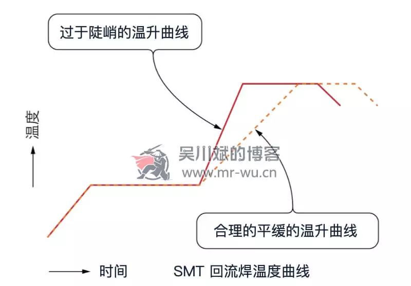
A steep temperature curve during reflow soldering, with a sudden temperature rise, can easily cause uneven temperatures at the pads of the component. A temperature rise rate of less than 2°C per second can help prevent tombstone issues.
Poor quality solder paste is another concern. Solder paste is an essential material in the reflow soldering process, consisting of a uniform mixture of alloy powder (particles) and a paste flux (rosin, thinner, stabilizers, etc.). The alloy particles are the main component that forms solder joints, while the flux removes the oxide layer on the soldering surface and improves wettability, making it a key material for ensuring solder paste quality. In terms of weight, solder paste is generally composed of 80% to 90% metal alloy, and in terms of volume, metal and flux each account for 50%.
Ensuring the quality of solder paste is primarily reflected in storage and usage. Solder paste is generally stored between 0°C and 10°C (or as required by the manufacturer). For usage, the environment in the SMT assembly workshop should be maintained at a temperature of 25±3°C and humidity of 50±10% (related to the characteristics of the solder paste). When using solder paste, it should be on a first-in, first-out basis, with proper usage records kept. The paste should be allowed to warm up for more than four hours, and it should be thoroughly stirred before use to ensure good printability and release properties. After adding solder paste, the inner and outer lids of the solder paste container should be closed immediately, and reflow soldering should be completed within two hours after printing.
These are all issues that SMT factories need to address. However, sometimes tombstone defects are quite severe, and the SMT side claims to have controlled the production process, shifting the blame to the layout. So how can we avoid tombstone defects during layout?
First, attention should be paid to reasonable pad design.
Pad design should strictly maintain symmetry, meaning that the shapes and sizes of the pads on both sides should be identical to ensure that the stress on both sides of the component is the same when the solder melts, avoiding tombstone phenomena.
SMT pad design is a very important aspect of PCB design, as it determines the soldering position of components on the PCB. A reasonable pad design allows for minor placement offsets during SMT, which can be automatically corrected during reflow soldering due to the surface tension of the molten solder. However, if the PCB pad design is unreasonable, the molten solder can cause uneven stress on both sides of the component, leading to defects such as component displacement or tombstone.
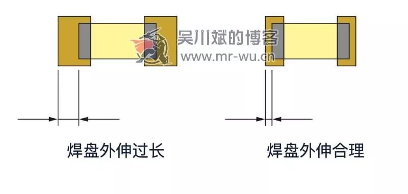
Short pad lengths for surface-mounted components can lead to displacement, open circuits, and soldering failures, while excessively wide pads can also cause component displacement and tombstone defects.
For creating packages, I recommend referring to the IPC-7351 standard. Most mainstream EDA software includes a package creation tool based on the IPC-7351 standard, which you should make good use of.
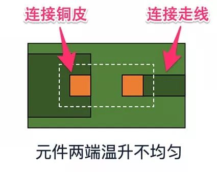
Pad connections to copper should be designed with flower pads to avoid large area copper connections that can cause uneven heating of the pads due to thermal vias.
Wiring should be symmetrical from the pad, and the width of the traces entering the pad should also be symmetrical.
Additionally, during PCB design, ensure that two components do not share the same pad.
Alright, save this article from Old Wu, so that when discussing with SMT, we have evidence and are not afraid of them passing the buck 😂