Test Coupon: Commonly known as Impedance Strip
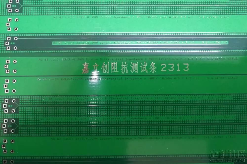
The Test Coupon is used to measure the characteristic impedance of the produced PCB using a TDR (Time Domain Reflectometer). The impedances that need to be controlled generally include single-ended lines and differential pairs, so the trace width and spacing (when differential pairs are present) on the test coupon must match those of the lines to be controlled. Most importantly, the location of the ground point during measurement is crucial. To reduce the inductance of the ground lead, the grounding point of the TDR probe is usually very close to the measurement signal point (probe tip), so the distance and method of measuring the signal point on the test coupon must comply with the specifications of the probe used.
Gold Finger
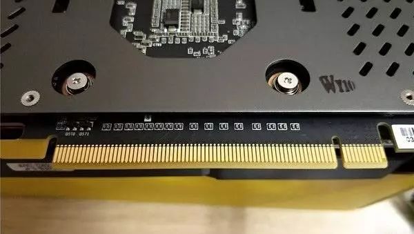
Here, the term Gold Finger does not refer to Kato Takashi. The purpose of the Gold Finger (Gold Finger, also known as Edge Connector) design is to create a conductive interconnection through pressure contact with the connector’s contact springs. Gold is chosen for its superior conductivity and oxidation resistance. The shiny gold strip on your computer’s memory module or graphics card is the Gold Finger.
Now the question arises, is the gold on the Gold Finger real gold? I believe it should be gold, but not pure gold. Why? Because pure gold is not hard enough. In historical dramas, those who verify if a gold ingot is real gold often bite it with their front teeth to see if there are bite marks. I don’t know if this is a scriptwriter’s fantasy, but Gold Fingers must withstand frequent insertion and removal, so instead of pure gold, they are generally plated with “hard gold”. Here, hard gold refers to an alloy (which is a combination of Au and other metals), making it harder.
Hard Gold, Soft Gold
Hard Gold: Hard Gold; Soft Gold: Soft Gold
Soft gold plating is achieved by electroplating nickel-gold onto the circuit board, with thickness control being relatively flexible. It is generally used for aluminum wire bonding on COB (Chip On Board) or the contact surfaces of mobile phone buttons, while the gold used for Gold Fingers or other adapter cards and memory is mostly hard gold, as it must be wear-resistant.
To understand the origins of hard gold and soft gold, it is best to first have a brief understanding of the gold plating process. Without discussing the earlier acid cleaning process, the basic purpose of electroplating is to deposit “gold” onto the copper foil of the circuit board. However, direct contact between “gold” and “copper” will cause a physical reaction of electronic migration diffusion (due to potential difference), so a layer of “nickel” must be plated first as a barrier layer, and then gold is plated on top of the nickel. Therefore, what we commonly refer to as gold plating should actually be called “nickel-gold plating”.
The difference between hard gold and soft gold lies in the composition of the final layer of gold plated. During gold plating, one can choose to electroplate pure gold or an alloy. Since pure gold is softer, it is referred to as “soft gold”. Because gold can form a good alloy with aluminum, COB requires a specific thickness of this pure gold layer when bonding aluminum wires.
Additionally, if one chooses to electroplate nickel-gold alloy or gold-cobalt alloy, the alloy will be harder than pure gold, hence it is referred to as “hard gold”.
Through Hole: Plating Through Hole (PTH)
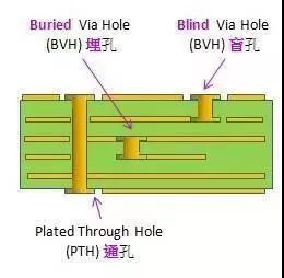
The copper foil lines between conductive patterns on different layers of the circuit board are connected using these holes, but they cannot be used for inserting component leads or other reinforcement materials. Printed Circuit Boards (PCBs) are formed by stacking multiple layers of copper foil. The copper foil layers cannot communicate with each other because each layer is covered with an insulating layer, so they need to rely on vias to link signals, hence the term “through hole” in Chinese.
Through holes are the simplest type of hole, as they can be made by directly drilling or using lasers to create full holes in the circuit board, making them relatively inexpensive. However, some circuit layers do not require these through holes, but if the vias are fully penetrated, it can lead to waste, especially for high-density HDI board designs where PCB space is at a premium. Therefore, while through holes are cheap, they can sometimes take up unnecessary PCB space.
Blind Hole: Blind Via Hole (BVH)
Blind holes connect the outermost layer of the PCB circuit to the adjacent inner layer through plated holes, and since they cannot be seen from the opposite side, they are called “blind holes”. To increase the space utilization of PCB circuit layers, the “blind hole” process was developed.
Blind holes are located on the top and bottom surfaces of the circuit board and have a certain depth, used to connect surface lines to the inner layer lines below. The depth of the hole generally has a specified ratio (hole diameter). This manufacturing method requires special attention; the drilling depth must be just right, as improper attention can lead to difficulties in plating the hole. Therefore, very few factories adopt this manufacturing method. In fact, it is also possible to pre-drill the holes needed for connection in individual circuit layers before bonding them together, but this requires precise positioning and alignment devices.
Bury Hole: Buried Via Hole (BVH)
A buried hole refers to the connection between any internal circuit layers of the printed circuit board (PCB) without connecting to the outer layer, meaning there are no vias extending to the surface of the circuit board.
This manufacturing process cannot be achieved by drilling after the circuit board is bonded; it must be done during the individual circuit layer operations, first partially bonding the inner layers and then performing plating treatment, followed by full bonding. Since this process is more labor-intensive than the original through holes and blind holes, it is also the most expensive. This manufacturing process is usually only used for high-density circuit boards to increase the space utilization of other circuit layers.