In the race towards high-speed and high-integration semiconductor chips, low-K (low dielectric constant) materials are undoubtedly the “unsung heroes”! Traditional silicon dioxide (k≈4) can no longer meet the demands for low power consumption and low latency in chips, while low-K materials (k<4) can perfectly address issues such as excessive capacitance between wires and leakage heat, making them one of the core materials for ultra-large-scale integrated circuits (ULSI). This comprehensive guide breaks down the classification, mainstream models, and selection techniques of low-K materials clearly, making it a handy reference for chip research, manufacturing, or procurement!
1. First, understand: How important are low-K materials?
As chip processes advance to the 10nm level, transistor density increases, and wire spacing decreases, traditional silicon dioxide as an interlayer dielectric leads to three major problems:
- Increased parasitic capacitance → signal transmission delay and severe crosstalk;
- Increased leakage current → skyrocketing chip power consumption and severe heating;
- Dielectric loss → affects chip stability and lifespan.
Low-K materials (k<4) and ultra-low-K materials (k<2) can fundamentally solve these problems by reducing the dielectric constant, making them the “best partners” for copper interconnect technology and indispensable core materials for advanced process chips!
2. Core Classification: Three Major Types of Low-K Materials, Easily Distinguishable Features
Low-K materials are mainly divided into three categories: organic, inorganic, and porous, each with mainstream representative models, distinct advantages, and application scenarios. Here’s a table for clarity:
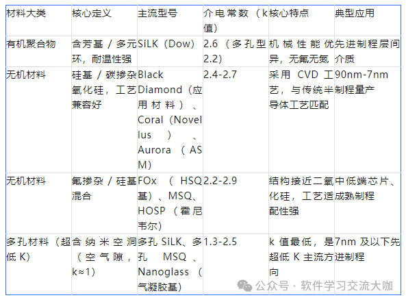
Key Point: Ultra-low K materials (k<2) can only be achieved through a “porous structure” because the dielectric constant of air is close to that of a vacuum (k≈1), which is currently the core idea for reducing k values!
3. In-depth Analysis of Mainstream Low-K Materials (Collectible Content)
1. Organic: SiLK Series (Dow Chemical)
- Standard SiLK: k=2.6, aromatic thermosetting material, free of fluorine/oxygen/nitrogen, with strong thermal resistance (can withstand over 400℃ crosslinking);
- Porous SiLK: k=2.2, incorporates nano-holes, with the best mechanical properties among porous materials, but at a higher cost;
- Applicable scenarios: Advanced process chips with high mechanical strength requirements, such as high-end CPUs and GPUs.
2. Inorganic: Carbon-Doped Silicon Dioxide (Most Mass-Produced)
- Representative models: Black Diamond (Applied Materials), Coral (Novellus), Aurora (ASM);
- Commonality: k=2.4-2.7, produced using chemical vapor deposition (CVD) process, perfectly compatible with traditional semiconductor processes, currently the most widely used low-K material;
- Special applications: Aurora is used by Intel in 90nm and 65nm production lines, while Black Diamond has become the first choice for mass production due to its stability.
3. Porous: Ultra-Low K Ceiling
- Porous MSQ: k=2.2-2.5, silicon-based material, structure similar to silicon dioxide, strong process compatibility, but mechanical properties are inferior to porous SiLK;
- Nanoglass (aerogel-based): k=1.3, currently reported as the lowest k material, launched jointly by Nanopore and Honeywell, with outstanding ultra-low dielectric advantages;
- Key process: Synthesizing nano-holes through block copolymerization or removing pore-forming agents after spin coating and heating to form a porous structure.
4. Selection Techniques + Pitfall Avoidance (A Must-Read for Chip Professionals)
1. Three Major Principles for Selection
- Process consideration: For advanced processes of 7nm and below → choose porous SiLK, Nanoglass (ultra-low K); for mature processes (90nm-28nm) → choose Black Diamond, Coral (carbon-doped silicon dioxide);
- Process method: For spin coating processes → choose SiLK, MSQ; for CVD processes → choose Black Diamond, Aurora;
- Demand consideration: For high mechanical strength requirements → choose SiLK series; for process compatibility priority → choose MSQ, carbon-doped silicon dioxide.
2. Two Key Points to Avoid Pitfalls
- Fluorine-doped materials (such as some inorganic low-K): Although they have low k values, they have poor moisture resistance, requiring good packaging protection to avoid moisture affecting performance;
- Porous materials: The more holes, the lower the k value, but the worse the mechanical strength and density, requiring a balance between dielectric constant and mechanical performance to avoid cracking during chip packaging.
5. Future Trends: Ultra-Low K Materials Become Core Track
As chip processes advance towards 3nm and 2nm, the requirements for dielectric constants become increasingly stringent (target k<2), and porous materials will become the absolute mainstream:
- Further reduce the size of nano-holes to enhance mechanical properties;
- Develop “defect-free porous structures” to reduce leakage risks;
- Optimize process compatibility to adapt to advanced manufacturing processes such as EUV lithography.
Interactive Time
What types of low-K materials have you used in chip research or production? Have you encountered issues with process compatibility or insufficient mechanical strength? Share your practical experiences in the comments, and I will help you analyze selection optimization solutions!
#low-K materials #semiconductor materials #chip manufacturing #integrated circuits #semiconductor processes #advanced processes #chip research