
Today, we mainly discuss: improvements in switch mode power supply design.
1. PCB Coupling
Engineers typically pay close attention to two coupling factors in SMPS layout, as shown in the figure below:
-
Voltage switching node, which has high dv/dt
-
Thermal current loop, which contains the highest di/dt in the subsystem
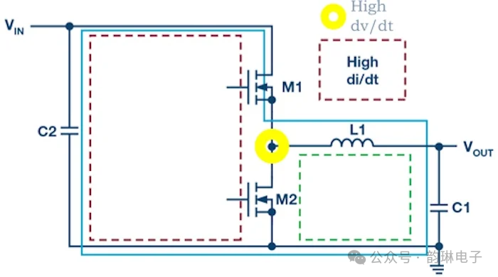
Diagram showing the di/dt and dv/dt positions of the buck converter
The mechanisms and risks at play here are dv/dt and di/dt
2. PCB Design Inspection
Here, we inspect the PCB layout of the LM22678 5A converter, with Uin at 12V and Uout at 5V. This is a synchronous buck converter using a B130L-13-F Schottky diode for its low-side switching element.
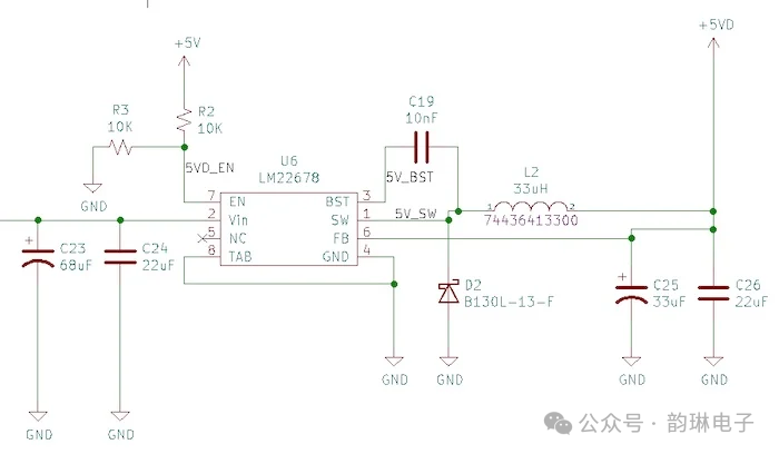
12V to 5V asynchronous LM22678 buck converter schematic
Minimizing capacitive and inductive coupling is not complex, but it is easily overlooked, leading to PCB issues and product delays.
In the figure below, the layout of the asynchronous buck regulator in a TO-263 package is shown, highlighting the voltage nodes (red outline) and thermal current loop (yellow).
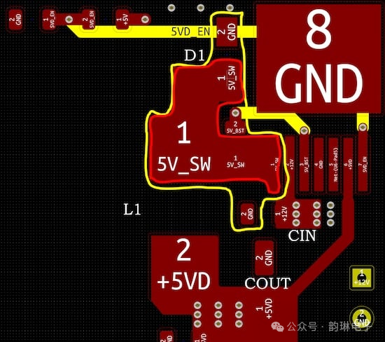
Design of an asynchronous buck regulator using a low-side power diode
To clarify, the copper fill on the PCB has been hidden, and this design has three obvious issues:
-
1. The high di/dt loop is much larger than necessary
-
2. No vias connecting the GND nodes of Cin or Cout (covered by vias)
-
3. The switching node could be smaller
This design indicates that the current loop is not well controlled, and due to the lack of vias between planes, the current does not have a clearly defined return path.
3. Regarding EMC
The improved layout is shown in the figure below:
-
Optimized voltage nodes, smaller thermal loops, and each passive component relative to the second layer reference plane.
-
Additionally, the primary Cout capacitor has also been rotated 90° compared to the original design, reducing noise risk on the input rail.
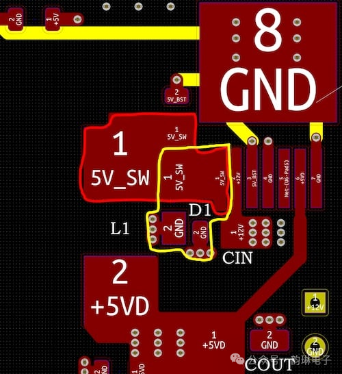
The improved layout considers coupling mechanisms
-
By moving the low-side diode in series between the switching pin and the inductor, potential crosstalk noise generated by dv/dt coupling effects can be better limited.
-
Furthermore, by reducing the geometry of the thermal loop, the impact of high di/dt magnetic field coupling can be reduced.
Although these changes are minor, they do not require additional PCB space or changes to other subsystems. However, by reducing the current loop by approximately 50% and optimizing nodes, system compliance has been enhanced.
4. Key Points
-
Understand the flow positions of current loops in switch mode power supplies
-
Keep node and loop geometries small to mitigate unnecessary coupling effects
-
Keep Cin away from or Cout to help isolate the current loop’s induced field and prevent dv/dt crosstalk
-
Connect pads to vias, not just ground fill copper, to help limit return current


Screenshots of some electronic books

【Complete Set of Hardware Learning Materials Collection】