Technical Coupling of PCB Manufacturing Processes and Electronic Chemicals
1. Process Differentiation between Reduction Method and Semi-Addition Method
In the reduction method process, blackening/browning treatment enhances interlayer adhesion by forming a nanoscale oxide layer (thickness about 0.5-1μm). After using a modified browning solution, a certain 8-layer PCB achieved an interlayer peel strength of 1.8N/mm; the semi-addition method (SAP) relies on etching process to control copper layer precision. A certain type of substrate manufacturer used a hydrogen peroxide-organic acid composite etching solution to achieve a line width tolerance of ±0.8μm at 15μm line width.
2. Equipment Iteration of Horizontal Electroless Copper Plating Process
The third-generation horizontal electroless copper plating equipment integrates pulse plating (frequency 100-200Hz) and intelligent temperature control (±0.3℃), achieving copper layer uniformity of ±5% in 12:1 aspect ratio vias, with a 40% efficiency improvement over traditional vertical electroless copper plating processes.
Breakthroughs in Chemical Technology for High-End PCB Processes
1. Blind Hole Treatment and Reliability Improvement
In the micro-gap (2-5μm) repair of laser blind holes (hole diameter 50μm), a certain HDI board manufacturer adopted a “expansion liquid + catalytic activation” combination process, achieving 100% coverage of the copper layer at the bottom of the blind hole, with no cracks after 1000 thermal cycles (-40℃~125℃). Automotive electronic PCBs require that the internal stress of the copper layer be <10MPa, which can be reduced to 6MPa by adding organic amine inhibitors.
2. High-Frequency and High-Speed Material Adaptation Technology
For PTFE substrates (Dk=2.65), after plasma (CF4/O2) and chemical micro-etching synergistic treatment, the bonding strength of the copper layer increased from 3N/cm to 5.2N/cm; in high-frequency and high-speed boards with a 10:1 aspect ratio, the surface tension of the optimized electroless copper solution decreased to 32mN/m, and the solution penetration time was shortened to 12 minutes.
3. Cutting-Edge Applications of Packaging Substrates
The SAP process electroless copper solution developed by Tiancheng Technology achieved a chemical copper layer roughness Ra < 0.8μm in 10/10μm line width substrates, verified by the Institute of Microelectronics of the Chinese Academy of Sciences, with performance comparable to that of Amtech products. After amino silane modification, the copper layer adhesion of ABF substrates increased to 4.8N/cm, meeting the requirements for flip-chip packaging.
Innovations in Environmental Protection and Cost Control Technology
1. Innovation of Nickel-Free Electroless Copper System
The cobalt-boron catalytic system achieves an electroless copper plating rate of 2.5μm/h, with wastewater nickel content <0.3mg/L; a certain company developed an electro-deposition recovery technology that increased the nickel ion recovery rate to 98%, reducing wastewater discharge by 80,000 tons annually.
2. Efficient Utilization of Palladium Resources
By optimizing the model of hole wall roughness and palladium adsorption amount, a certain HDI board manufacturer reduced the palladium sulfate consumption from 153.2g / 10,000㎡ to 128g / 10,000㎡, saving material costs by 3 million yuan annually in conjunction with online regeneration technology.
Industry Development Trends and Localization Progress
1. Cutting-Edge Technological Directions
By 2025, mass production of 5/5μm line width packaging substrates is expected, requiring the development of nanoscale copper particle (particle size <50nm) electroless copper solutions; AI process systems have achieved a copper solution lifespan prediction error of <3%, promoting fully automated production.
2. Breakthroughs in Domestic Substitution
The market share of domestic companies in the chemical field for high-frequency and high-speed boards increased from 15% in 2020 to 28% in 2023, with ultra-coarse products from companies like Tiancheng Technology and Banming Technology being introduced into high-end PCB production lines such as Jingwang Electronics and Nanya Circuits.
Analysis of Typical Application Scenarios
1. 5G Base Station PCB
Using Rogers RO4835 substrate (Dk=3.0, Df=0.0023), combined with horizontal electroless copper plating + pulse plating process, signal loss of <0.3dB/in was achieved in the 28GHz frequency band, with via copper thickness uniformity of ±2.5%.
2. Automotive Millimeter-Wave Radar Board
The 77GHz radar PCB adopted the semi-addition method + etching process, controlling the line width at 12μm±1μm, with impedance deviation <3% after 1000 hours of high temperature and humidity (85℃/85% RH) testing.
3. Semiconductor Test Substrate
A certain 12-layer test substrate used ion palladium activation + low-stress electroless copper solution, achieving copper thickness of 25μm±1μm in 15:1 aspect ratio vias, capable of withstanding 500 thermal shock cycles (-55℃~125℃) without failure.
Future Technology Roadmap Planning
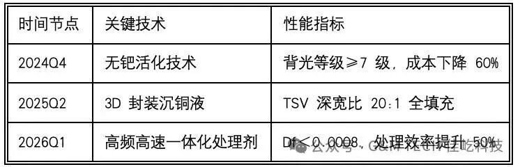
Electronic chemicals specifically for PCBs are evolving along the path of “high precision, low loss, and greening”. Domestic companies need to deepen breakthroughs in material molecular design and process intelligent control to achieve full-chain localization of high-end products.

Jia Yi Technology

Official Website | gmtechcn.com
Sales Department Email | sale@gmtechcn