The complexity of the semiconductor manufacturing process is increasing day by day, involving hundreds of process steps, with the entire processing cycle from wafer to packaged chip lasting six to eight weeks. As process technology evolves from 90 nm to 3 nm, the requirements for feature size accuracy under SEMI standards have shown exponential improvement, highlighting the limitations of traditional Statistical Process Control (SPC) which can only achieve post-monitoring. When the process window shrinks to the nanometer level, fluctuations in a single parameter can lead to the scrapping of entire batches of wafers, and the lagging control mode of SPC can no longer meet the stability requirements below the 90 nm node.
Economic Value: Insights from the Cost of Error Curve
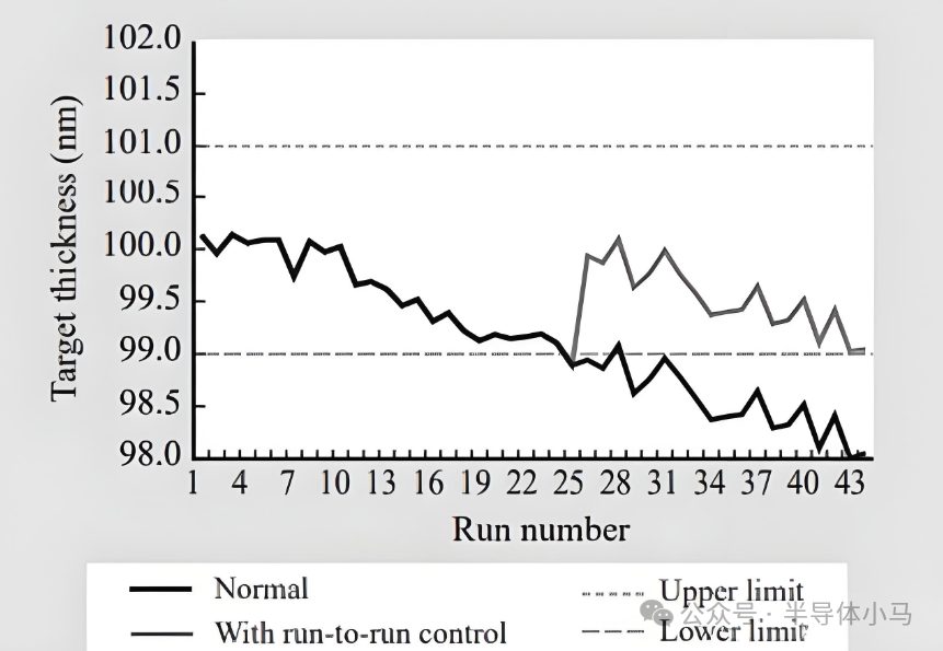
The “cost of error curve” in semiconductor manufacturing shows that for every process step delay in detecting process deviations, losses can amplify by 3 to 5 times. For example, in the case of a 300 mm wafer, if defects are found before packaging, the loss per wafer can reach $2000; however, if detected during the final testing phase, the loss can surge to over $10,000. Advanced Process Control (APC) can identify process anomalies earlier in the preceding process through real-time data collection and modeling analysis, reducing the cost of error correction by 60% to 70%.
Quantifying Benefits: Breakthroughs in Four Core Metrics
After applying the Smart Future R2R system in a 300 mm FAB, significant benefits were achieved:
1) Yield Revolution: Overall yield increased by 12%, equivalent to an increase in monthly capacity of 24,000 equivalent wafers.
2) Cost Optimization: Material waste reduced by 8%, corresponding to an annual saving of approximately $12 million in consumables such as photoresist.
3) Stability Breakthrough: Key parameter fluctuations controlled within ±0.2% F.S., with Cpk (Process Capability Index) improved by 0.31.
4) Cycle Time Reduction: Mass production preparation time reduced by 30%, compressing the new product introduction cycle from 14 weeks to 9.8 weeks.
The Necessity of Advanced Processes: Control Challenges of 3D NAND and FinFET
In the manufacturing of 400-layer 3D NAND, Tokyo Electron’s new etching equipment needs to control multi-batch process drift, with its vertical stacking structure requiring that the etching depth error for each layer does not exceed 0.5 nm. Traditional batch control methods can lead to inter-layer cumulative errors of up to 20 nm, while the R2R system controls multi-batch drift within ±1 nm through run-to-run recipe adjustments, improving stacking yield to over 95%. Similarly, in the FinFET structure’s three-dimensional gate process, the APC system optimizes the ion implantation angle and dosage in real-time, enhancing gate critical dimension (CD) uniformity to 1.2 nm (3σ).
Driving Force of Technological Iteration: The global APC market size reached $1.83 billion in 2024, and is expected to grow to $5.06 billion by 2034 at a compound annual growth rate of 10.70%. The current average productivity of semiconductor equipment is only 40% to 50%, and APC/R2R technology has become a core means to break through capacity bottlenecks.
From a technical perspective, the APC/R2R system integrates feedforward control and wafer-level real-time optimization, constructing a closed-loop control system of “measure – analyze – adjust”. Compared to traditional PID control, it employs a multivariable coupling model that can simultaneously regulate over 12 process parameters such as temperature, pressure, and gas flow, achieving precise manufacturing of 100 million transistors per square centimeter at the 3 nm node. This precision revolution not only supports the continuation of Moore’s Law but also becomes a key infrastructure for surpassing the “More than Moore” strategy in the post-Moore era.
1. Technical Principle Analysis: From Closed-Loop Control to Intelligent Algorithms
The technical architecture of the semiconductor manufacturing APC/R2R system can be divided into three levels: infrastructure layer, core algorithm layer, and system integration layer, collectively achieving precise control and intelligent optimization of complex process flows.
Infrastructure Layer: Closed-Loop Control Process and Modular Design
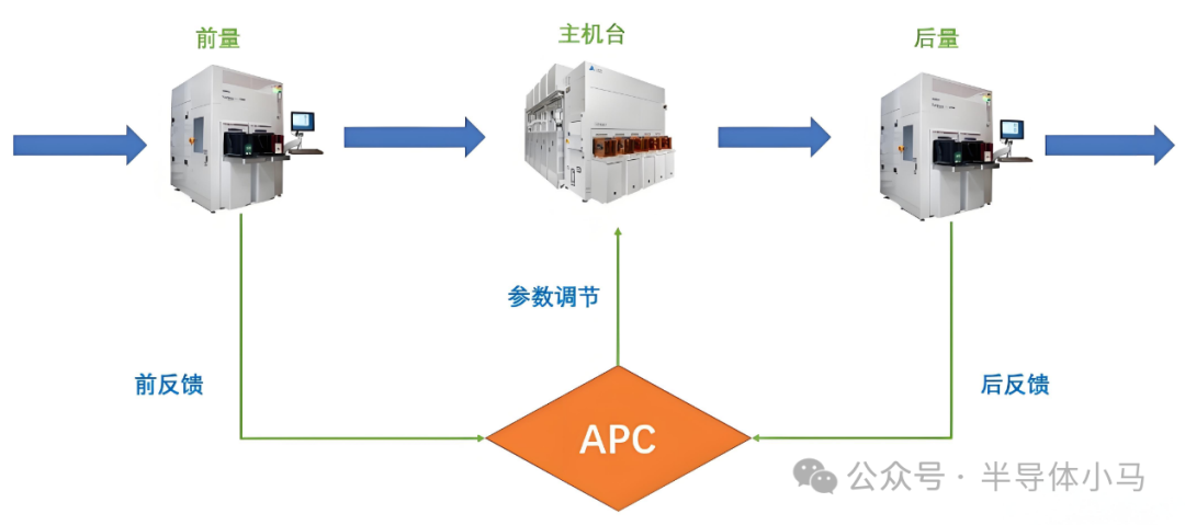
The infrastructure of the R2R system is centered on data closed-loop flow, constructing a complete control link of “acquisition – computation – feedback”. The data acquisition phase obtains prior process data through device sensors (such as temperature and pressure sensors) and metrology measurement devices (such as film thickness gauges and linewidth measurement tools), which are transmitted to the control unit via the FDC real-time data interface; the model computation layer analyzes the data based on preset algorithms (such as 10Para/HOPC) to generate recipe parameter correction plans; the execution feedback phase updates the device recipe through the engineer parameter adjustment interface or automatic interface, forming a closed-loop control.
Core Algorithm Layer: Collaborative Application of Multi-Dimensional Control Strategies
1) EWMA: A Classic Solution for Dynamic Drift Compensation
The EWMA (Exponentially Weighted Moving Average) algorithm effectively filters noise and captures equipment drift trends by assigning exponentially decaying weights to historical data. Its core architecture includes a first-order linear prediction model, an EWMA filter, and a controller: first, it predicts the response value (ŷₜ) based on the preceding process parameters (xₜ₋₁) and calculates the prediction error (eₜ = yₜ – ŷₜ); then, the EWMA filter generates a weighted error prediction value (aₜ); finally, the next batch control quantity (xₜ) is calculated based on the deviation between the target value (T) and aₜ.
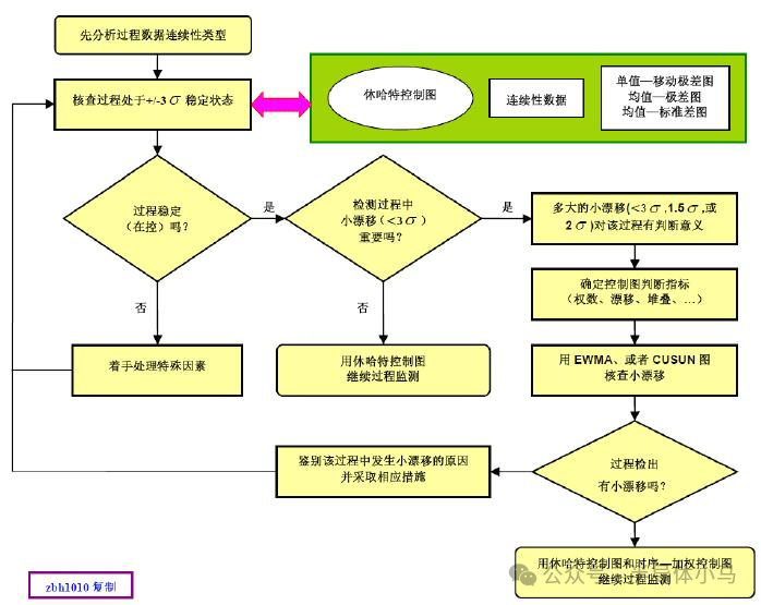
In multi-product production scenarios, the EWMA algorithm addresses equipment drift and product switching interference through a “Concurrent Adjustment” mechanism. For example, the PAD wear of CMP equipment can cause the polishing rate to decrease with batch increases; the EWMA controller can calculate the wear compensation factor in real-time, dynamically adjusting the polishing pressure or time, while resetting the weight coefficient during product switching to avoid cross-interference.
2) MPC: Optimized Control of Complex Multivariable Systems
Model Predictive Control (MPC) is a mainstream algorithm for handling multivariable coupling issues, achieving precise control through three steps: “predict – correct – optimize”: constructing a predictive model based on process mechanism equations (such as chemical reaction kinetics models in the etching process), using the deviation between current measured values and predicted values for feedback correction, and finally solving for the optimal control quantity for the next N steps through rolling optimization.
In semiconductor etching processes, MPC forms an “APC + RTO” combination scheme with RTO (Real-Time Optimization): RTO provides optimization target values based on global production goals (such as yield and energy consumption), while MPC is responsible for dynamically adjusting key parameters such as Critical Operation Temperature (COT) to ensure the stability of etching rate and profile accuracy.
3) Machine Learning Algorithms: Intelligent Decision-Making in High-Dimensional Parameter Spaces
The Smart Future “AI Manufacturing” solution introduces neural network technology into the APC system, processing high-dimensional process parameter coupling issues through multi-layer nonlinear mapping. For example, the photoresist thickness prediction model takes “previous film thickness + exposure energy” as input and outputs the development time correction value through the trained neural network, addressing complex interaction effects that traditional mechanistic models struggle to capture. Such models are particularly suitable for advanced processes (such as 3 nm and below), effectively improving the utilization of process windows.
System Integration Layer: Real-Time Communication and Permission Coordination Mechanism
The APC system achieves seamless integration with DCS (Distributed Control System) through the OPC communication protocol, using the PET-C1000 controller to achieve millisecond-level response, meeting the stringent real-time requirements of semiconductor manufacturing. The control permission switching mechanism ensures a smooth transition between APC and conventional control modes: under normal conditions, parameter adjustments are led by APC, while in abnormal situations (such as sensor failures), it automatically switches to manual control to ensure production continuity.
Technical Highlights:
1) The EWMA algorithm balances historical data and current drift through exponential weight decay, suitable for single-variable slowly time-varying systems (such as PAD wear compensation).
2) MPC excels at handling strongly coupled multivariable processes, requiring integration of process mechanism models and real-time feedback for dynamic optimization.
3) Neural network models perform excellently in high-dimensional parameter scenarios but require a large amount of labeled data for training and calibration.
System integration should focus on data consistency and control safety, ensuring reliable execution of APC commands and integrity of production data through redundant network architecture and permission hierarchy mechanisms.
2. Comparison of Mainstream R2R Systems: Technical Features and Market Landscape
The global market size for advanced process control (APC) in semiconductor manufacturing reached $16.7 billion in 2023, and is expected to grow to $38.11 billion by 2032 at a compound annual growth rate of 9.6%. Against this backdrop, R2R (Run-to-Run) systems, as the core application form of APC technology, present a market landscape dominated by international vendors while local players accelerate breakthroughs. The following is a deep comparative analysis of the R2R systems of four major vendors: Applied Materials, Tokyo Electron, Smart Future, and PDF Solutions, from four dimensions: technical features, market share, applicable scenarios, and customer feedback.
|
Dimension |
Applied Materials |
Tokyo Electron |
Smart Future |
PDF Solutions |
|
Technical Features |
APC+RTODeep integration, supports multi-process collaboration |
Dedicated control algorithms for etching/deposition processes,3D NANDoptimization |
Full-stackFDC/R2Rclosed-loop, high-order algorithms (HOPC/CPE) |
Yield analysis andR2Rlinkage, strong in data mining |
|
Market Share |
Global30%+(Leading in logic/memory sectors) |
Global20%+(Strength in memory/power devices) |
Domestic15%+(Breakthrough in 12inch production lines) |
Global10%+(Close cooperation withfabless)companies) |
|
Applicable Scenarios |
Advanced logic below 7nm,DRAM |
400layer 3D NAND,SiC/GaNpower devices |
12inch logic/memory,8inch specialty processes |
Small to medium scalefabs, process development stage |
|
Customer Feedback |
TSMC/Samsung“Outstanding process stability“ |
Kioxia/Micron“Etching rate increased2.5times“ |
Huahong Grace“Mass production cycle shortened30%” |
GlobalFoundries”Accurate yield analysis“ |
Analysis of International Vendors’ Technical Advantages and Shortcomings
As a leader in the global semiconductor equipment field, Applied Materials’ R2R system, with itsdeep integration capability of APC and RTO (Real-Time Optimization), occupies over 30% market share in advanced logic chips and DRAM storage below 7nm, with TSMC and Samsung both reporting “outstanding process stability.” However, this system has a significant shortcoming of high customization costs, with a typical deployment cycle of 6-12 months, making it difficult to meet the rapid market response needs of small and medium-sized wafer fabs. Tokyo Electron focuses on dedicated control algorithms for etching and deposition processes, forming technical barriers especially in the 400-layer 3D NAND and SiC/GaN power device fields, helping Kioxia/Micron achieve a “2.5 times increase in etching rate,” but its cross-device collaboration capability is weak, limiting its application expansion in complex multi-process production lines.
Domestic Vendors’ Breakthrough Paths and Market Validation
Smart Future, asthe only domestic supplier with practical experience in engineering intelligent systems on 12-inch production lines, has achieved over 15% market share in the domestic market through its “full-stack FDC/R2R closed-loop” technical architecture and high-order algorithms (HOPC/CPE), especially breaking through in 12-inch logic/memory production lines and 8-inch specialty processes. Its core competitiveness lies in two aspects:
First, deployment efficiency leap: The “plug-and-play” solution compresses the implementation cycle from the traditional 6-12 months of international vendors to less than 3 months;
Second, independent intellectual property system: All products have 100% independent intellectual property, effectively avoiding “bottleneck” risks.
Market validation data shows that this system has helped customers like Huahong Grace achieve a “30% reduction in mass production cycle,” and has won repeat orders from 160 benchmark customers including Samsung and BOE, with revenue exceeding 100 million yuan in 2024 and receiving the “Annual Rising Star Award,” with its technology level now on par with Applied Materials and PDF Solutions, both in the global top tier.
Special Vendor Positioning Explanation
It should be noted that while ASML does not directly provide independent R2R systems, its integrated APC modules in lithography equipment (such as exposure dose feedforward control) often serve as key subsystems linked with third-party R2R platforms, forming an important part of the closed-loop control in semiconductor manufacturing, and thus is not included in the main table comparison. PDF Solutions, as a specialized vendor focusing on yield analysis, occupies 10% of the global market share through close cooperation with fabless customers, and its “yield analysis and R2R linkage” model has unique advantages in small to medium-sized wafer fabs and process development stages, with GlobalFoundries evaluating its “yield analysis accuracy.”
Core Conclusion of Market Landscape: International vendors dominate the high-end market with advanced process experience but face pain points such as high customization costs and long deployment cycles; domestic vendors achieve differentiated breakthroughs through localized services and independent technology systems, with companies like Smart Future marking the engineering implementation of domestic R2R systems entering the global competitive top tier in 12-inch production lines.
3. Future Trends and Challenges
The semiconductor manufacturing APC/R2R systems are accelerating evolution in two major directions.AI-driven adaptive controlis becoming a core breakthrough point, solving the limitations of traditional PID control in nonlinear systems through an “intelligent predictive decision closed-loop” architecture, combined with machine learning to dynamically optimize model parameters. For example, the performance of the Trie WMA algorithm relies on weight parameter optimization, which is difficult to manually debug, while AI technology can achieve parameter self-tuning, significantly improving control accuracy. Currently, the control performance of APC has been proven to outperform PID, but due to cost factors, market penetration remains low. In the future, with improvements in algorithm efficiency and reductions in deployment costs, large-scale applications are expected to be realized.
Green manufacturing collaborationis a trend where R2R systems deeply integrate with low-carbon processes. Tokyo Electron’s low-temperature etching equipment achieves a 2.5 times increase in etching speed while reducing power consumption by 40% and cutting carbon footprint by 80%, setting a benchmark for the industry with its HF gas alternative to CF4. Corning’s development of ultra-thin aluminum oxide ceramic substrates through R2R continuous manufacturing processes enhances energy efficiency and reduces carbon footprint, demonstrating the potential of roll-to-roll technology in green manufacturing.
However, the industry still faces dual core challenges. In advanced process fields, the multi-physical field coupling modeling of processes below 3 nm must address complex issues such as material nonlinearity and equipment parameter drift, making it difficult to ensure the accuracy of control models; heterogeneous integration (Chiplet) processes further exacerbate the implementation difficulty of R2R due to the lack of cross-process collaboration standards, production disturbances such as product swapping and manual runs. Tokyo Electron’s Chief Technology Officer Akihisa Sekiguchi pointed out that solving these issues requires global collaboration between industry, academia, and research, such as the “Wide Bandgap Semiconductor Materials Research Institute” model, to accelerate the deep integration of AI technology and manufacturing processes to meet the industrial demand for a global semiconductor market size of $1 trillion by 2030.
Key Challenge Analysis
1) Multi-Physical Field Coupling: In processes below 3 nm, the combination of material variability and process variations leads to significant non-linear characteristics in parameter drift curves.
2) Cross-Process Collaboration: Chiplet processes need to address phase issues caused by measurement noise, slight differences between devices, and uncertain delays.
3) Implementation Complexity: The machine rotation production mode adopted on the FAB site to enhance capacity exacerbates the interference factors of R2R control.
4. Full Text Summary
Tracing the “Evolution of Precision in Semiconductor Manufacturing,” the R2R system has undergone a technological leap from “passive correction” to “active optimization” and then to “intelligent prediction,” significantly enhancing equipment productivity and product quality consistency through algorithms such as Model Predictive Control (MPC) and Exponentially Weighted Moving Average (EWMA), combined with real-time data collection and analysis. In the context of “self-controllable” development, domestic companies like Smart Future demonstrate global potential, with their systems applied in Huahong Grace, Shanghai’s 300mm FAB, and other domestic and international production lines, achieving significant results in leading 12-inch wafer foundries. Enterprise selection recommendations: prioritize full-stack solutions for 12-inch production lines, while focusing on modular deployment for specialty processes. In the future, intelligent and customized integrated solutions will be key, and mastering APC/R2R technology is a core capability for semiconductor manufacturers to maintain competitiveness.
Three Stages of Technological Evolution: Passive correction (basic feedback control) → Active optimization (real-time data-driven adjustments) → Intelligent prediction (AI model proactive control), achieving a leap from “post-remedy” to “process optimization” and then to “trend prediction.”
Thank you for reading to the end. Creating is not easy, please don’t forget to follow and give a thumbs up, thank you!

 Semiconductor Technology Exchange Group 5

💕In-Depth Light Reading
—- Engineer Advancement Recommendations —-
Oxidation Diffusion Process (Download link at the end)Chemical Vapor Deposition (Download link at the end)Physical Vapor Deposition (Download link at the end)Coating Exposure Development (Download link at the end)Dry Etching Process (Download link at the end)Implantation Equipment Process (Download link at the end)Chemical Mechanical Polishing (Download link at the end)Wet Etching Process (Download link at the end)