This is the 248th original article by a lifelong learner.
What do the three generations of semiconductor materials refer to?
A semiconductor is a material that has electrical conductivity between that of a conductor and an insulator at room temperature. Common semiconductors include silicon, germanium, and compound semiconductors such as gallium arsenide, indium phosphide, gallium nitride, and silicon carbide.From the perspective of the generational development of semiconductor materials, they can be divided into three main stages.
First, it is important to understand that although the substrate materials of semiconductors have changed, the process of manufacturing chips based on these materials is quite similar. It starts with raw materials, which are first shaped into cylindrical forms and then sliced into thin wafers like cutting ham. These wafers are then divided into many small square grids, where chips are “sculpted” through steps such as photolithography, etching, and cleaning. Finally, these small grids, which are the chips, are cut out, packaged, tested, and made ready for use.
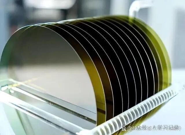
Wafer
1. First Generation Semiconductor Materials
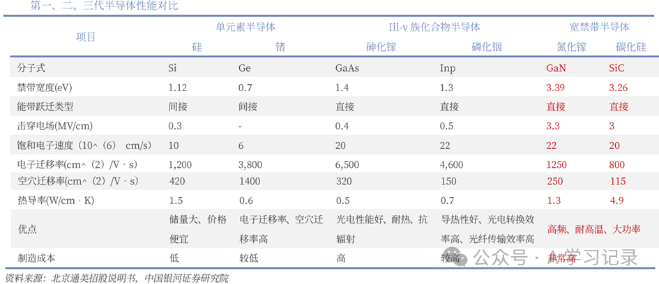
The first generation of semiconductor materials mainly refers to silicon (Si) and germanium (Ge).
In the early 1950s, germanium was the primary semiconductor material, widely used in space satellite solar panels due to its high electron mobility, high hole mobility, and low cost. However, it has the disadvantage of poor high-temperature resistance and radiation resistance.
After 1960, silicon became the main material. Although we have now developed to the third generation of semiconductors, most semiconductor chips and devices are still produced using silicon wafers as the substrate functional material. Silicon is stable, easy to obtain, abundant, and low-cost, primarily used in large-scale integrated circuits. However, it has a narrow bandgap and low electron mobility, which cannot meet the demands of high-frequency, high-power devices and optoelectronic devices.
2. Second Generation Semiconductor Materials
The second generation of semiconductor materials mainly refers to gallium arsenide (GaAs) and indium phosphide (InP).
Since the 1990s, with the rapid development of mobile information and the rise of the optical communication industry, the second generation of semiconductors represented by gallium arsenide and indium phosphide has begun to emerge and become popular.
The electron mobility of second-generation semiconductors is 4-8 times that of first and third-generation semiconductors, resulting in lower losses at the same current, making them suitable for high-frequency and high-speed environments. Among them, GaAs is widely used in LEDs, displays, and RF modules due to its good optoelectronic performance, heat resistance, and radiation resistance; InP is widely used in 5G base station optical modules and lidar due to its good thermal conductivity, high optoelectronic conversion efficiency, and high optical fiber transmission efficiency.
3. Third Generation Semiconductor Materials
The third generation of semiconductor materials mainly refers to gallium nitride (GaN) and silicon carbide (SiC).
Since the 21st century, the demand for high-power, high-voltage, and high-frequency electronic components in modern industry has surged, leading to higher requirements for the physical properties of semiconductor materials, such as bandgap width. The third generation of wide bandgap semiconductor materials, centered around silicon carbide and gallium nitride, has emerged. Although the manufacturing cost of third-generation semiconductor materials is relatively high, they are still widely used in various emerging fields due to their performance advantages. Among them, silicon carbide has developed rapidly with the rise of renewable energy.
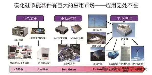
Gallium nitride (GaN) is mainly used in medium and low voltage applications, with fast switching speeds and high-frequency characteristics that allow for smaller inductors/capacitors, reducing system size, making it suitable for fast charging, 5G base stations, and RF devices. For example, many mobile phone chargers now use gallium nitride semiconductor materials.
Silicon carbide (SiC) can withstand voltages of over 1200V and can operate stably at temperatures above 175°C, making it suitable for applications such as electric vehicle main drive inverters, photovoltaics, and rail transportation. Currently, in addition to traditional application scenarios, silicon carbide materials can also be used in power supply units for AI data centers to reduce energy consumption, and can also be used in optical waveguide lenses for AI glasses to achieve a larger field of view and a simpler full-color display structure.
4. Detailed Comparison of Gallium Nitride and Silicon Carbide
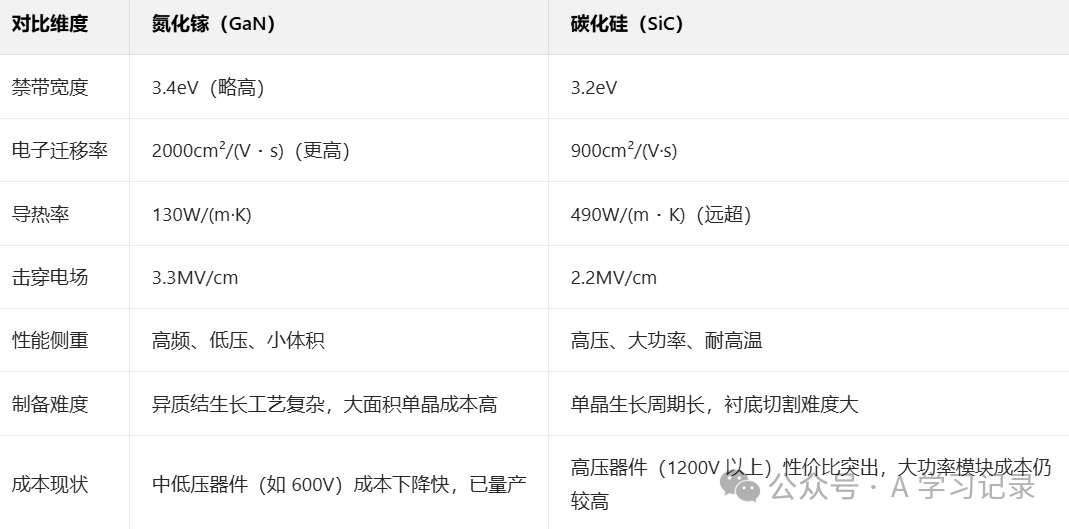
The main difference between GaN and SiC can be summarized in one sentence: GaN is more suited for “high frequency and low voltage,” while SiC is more suited for “high voltage and high power,” with each having its own application focus.
Compared to silicon-based semiconductors, both have some common core advantages:
-
Wide bandgap (GaN about 3.4eV, SiC about 3.2eV, silicon only 1.1eV): The breakdown electric field strength is 5-10 times that of silicon, allowing for higher voltage tolerance and smaller device size.
-
High thermal conductivity: SiC has a thermal conductivity of about 490W/(m・K), GaN about 130W/(m・K), both far exceeding silicon (150W/(m・K)), providing excellent heat dissipation performance suitable for high-temperature environments.
-
High-temperature resistance: Can operate stably at 200-600°C without complex cooling systems, reducing equipment weight and cost.
-
Low conduction loss: Fast switching speeds and higher energy conversion efficiency, especially suitable for high-frequency and high-power scenarios.
However, each also has some unique advantages:
Gallium nitride (GaN) has outstanding high-frequency performance, with an electron mobility of about 2000cm²/(V・s), which is 5 times that of silicon, and faster switching speeds than SiC, making it suitable for ultra-high-frequency scenarios; high device integration can be achieved through heterojunctions (such as AlGaN/GaN), resulting in very low on-resistance and smaller device sizes; efficiency is particularly good in low-voltage scenarios below 600V, balancing energy conversion efficiency and cost effectively.
On the other hand, silicon carbide (SiC) has stronger high-voltage capabilities, with a breakdown electric field strength of about 2.2MV/cm, slightly lower than GaN (3.3MV/cm), but with better stability in actual high-voltage scenarios (above 1200V); top-notch thermal performance: a thermal conductivity of 490W/(m・K) close to that of copper, making it the “heat dissipation king” in high-temperature and high-power scenarios; high mechanical strength: strong chemical stability and radiation resistance, suitable for harsh environments (such as aerospace and extreme industrial scenarios).
The comparison between the two is as follows:
Due to their core performance advantages, gallium nitride (GaN) is mainly used in consumer electronics, such as fast-charging chargers (for mobile phones, laptops), RF devices (mobile phone RF front ends); in the communication field, 5G base station power amplifiers (PA), microwave communication devices, satellite communication equipment; in the industrial and automotive fields, medium and low voltage inverters (such as 400V new energy vehicle OBC), low-voltage motor drives.
Silicon carbide (SiC) is mainly used in high-voltage inverters (800V platform) in new energy vehicles, on-board chargers (OBC), DC-DC converters, reducing energy consumption and improving range. Currently, almost all 800V models use silicon carbide, and as new energy vehicles gradually enter the 800V+ era, silicon carbide is becoming a necessary option; in the energy field, photovoltaic inverters, wind power converters, high-voltage transmission and distribution equipment (such as IGBT replacements); and in extreme environments, aerospace devices, rail transit traction converters, industrial high-temperature sensors, etc. In the future, it may also be increasingly used in AI chips, AI glasses, and other fields.
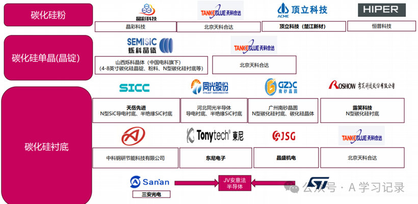
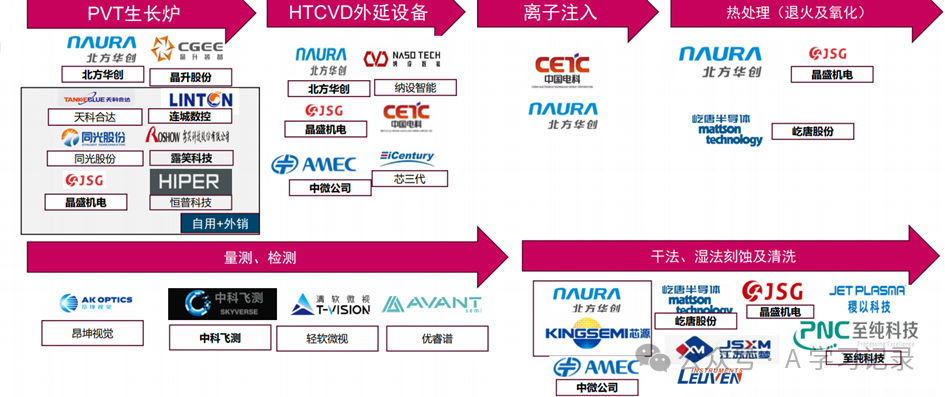
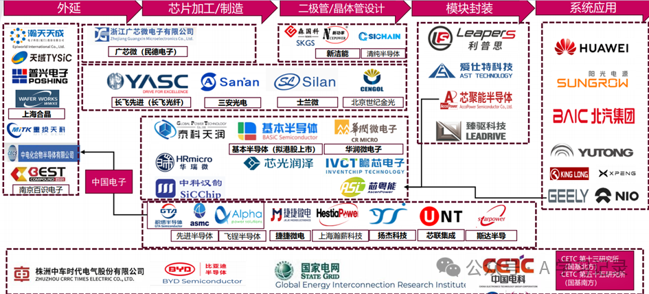
The silicon carbide industry chain is as follows: