Previously, we thoroughly understood the core practical points of grinding, such as Chuck Table Base Position calibration. Now, we must keep pace with industry trends—semiconductor grinding technology is undergoing explosive upgrades towards “greater precision, intelligence, and environmental friendliness”! Whether it’s advanced process chips, third-generation semiconductors, or high-end packaging demands, all are driving continuous breakthroughs in grinding technology. This trend analysis, combining industry reports and the latest technological developments, clearly breaks down the core directions, allowing newcomers to master them in advance and significantly enhance their workplace competitiveness.
Trend 1: Extreme Precision—Sub-Nanometer Level Flattening and Ultra-Thin Breakthroughs
As chip processes enter the 2nm era, the precision requirements for grinding have jumped from “nanometer level” to “sub-nanometer level,” while ultra-thin wafers have become mainstream in packaging. These two breakthroughs are particularly critical:
- New Record for Flatness: Advanced processes require global flatness of wafers to be within 0.5nm (2nm process standard), far exceeding the traditional ±5μm TTV control, necessitating comprehensive upgrades in Chuck Table calibration, grinding wheel precision, and polishing liquid formulations—such as using “multi-zone pressure control” technology to ensure that the grinding pressure error in different wafer areas is ≤±5kPa, avoiding local depressions or protrusions;
- Normalization of Ultra-Thin Wafers: 3D packaging and Chiplet technology are pushing wafer thickness down to below 20μm (even at the 10μm level). Traditional vacuum suction is prone to cracking, now relying on “flexible grinding pads + temporary bonding/debonding technology,” combined with micro-stress adsorption design of the Chuck Table, reducing the breakage rate from 3% to below 0.1%;
- Key Indicators: Surface roughness Ra < 0.1nm (atomic-level flatness), thickness tolerance ±0.5μm (3σ), has become the “passing line” for mid-to-high-end chip grinding.
Key Point: Future newcomers must master the skill of “sub-nanometer precision calibration,” such as laser-assisted dynamic calibration of the Chuck Table, to meet advanced process requirements.
Trend 2: Diversification of Material Adaptation—Third-Generation Semiconductors and Heterogeneous Integration Response
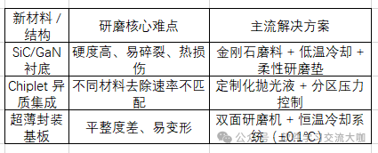
Traditional silicon wafer grinding can no longer meet market demands; grinding technology for new materials and complex structures has become a core competitive advantage:
- Special Breakthroughs in Third-Generation Semiconductors: SiC (silicon carbide), GaN (gallium nitride), and other wide bandgap materials have high hardness and brittleness, requiring a combination of “diamond abrasives + low-temperature cooling liquids” for grinding, ensuring processing efficiency (material removal rate increased by 20%) while avoiding micro-cracks—such as SiC substrate grinding achieving a thickness ≤100μm, with a 30% reduction in conduction resistance, suitable for power devices in new energy vehicles;
- Heterogeneous Integration Mixed Grinding: Chiplet packaging requires precise polishing of different materials (silicon, copper, silicon nitride) on the same wafer, promoting the development of “customized polishing liquid formulations,” such as a selection ratio of copper to silicon nitride exceeding 100:1, avoiding damage to sensitive layers during grinding;
- Upgrading of Packaging Substrate Grinding: Grinding of metallization layers on BT resin and ceramic substrates requires controlling surface roughness Ra < 0.05μm to ensure circuit interconnection without signal interference, relying on the dual-disk synchronous processing technology of high-precision double-sided grinders.
Trend 3: Equipment Intelligence—AI + Digital Twin Empowering the Entire Process
Grinding equipment is upgrading from “manual calibration” to “intelligent autonomous decision-making,” significantly lowering the operational threshold for newcomers:
- AI Parameter Self-Optimization: Equipment integrates AI algorithms to monitor the surface morphology of wafers and grinding wheel wear status in real-time, automatically adjusting the Chuck Table angle, grinding pressure (±0.01MPa precision), and feed speed. For example, Anji Technology’s AI polishing system improves rate stability by 15%;
- Digital Twin Simulation Prediction: Virtual simulations recreate grinding scenarios, predicting wafer warping and micro-crack risks in advance. For different thickness wafers, the best adsorption parameters for the Chuck Table are simulated, reducing actual trial-and-error costs;
- Real-Time Monitoring Closed Loop: Grinding machines integrate laser thickness gauges and online AOI detection modules, refreshing data every 10ms. If thickness deviation exceeds 0.1μm, the machine immediately stops for adjustment, improving yield from 85% to 98%.
Avoid Pitfalls: Newcomers should no longer rely on “experience-based parameter adjustments”! In the future, it is essential to master the basic operations of the AI parameter system, such as checking grinding wheel wear warnings and adjusting pressure zone parameters.
Trend 4: Green Manufacturing—Energy Saving and Waste Reduction + Recycling as a Necessity
Driven by environmental policies and cost control, grinding processes are transitioning to “low pollution, high recycling”:
- Recycling and Reusing Grinding Liquids: Using a “multi-stage filtration + ion exchange” system, the recovery rate of grinding liquids exceeds 90%, reducing chemical waste discharge while lowering procurement costs (annual savings of 30% on consumables);
- Dry Grinding Technology Popularization: For thermally sensitive products, dry polishing replaces traditional wet grinding to avoid contamination from residual grinding liquids, with energy consumption reduced by 40%. Currently, its application in chips below 28nm accounts for 25%;
- Green Upgrading of Consumables: Polishing liquids use biodegradable chemical active ingredients, and grinding wheels utilize recycled diamond particles, complying with ISO 14001 environmental standards while reducing resource waste.
Trend 5: Process Integration—One-Stop Processing + Composite Process Efficiency
The traditional segmented process of “grinding → cleaning → inspection” has been disrupted, with integration and composite processes becoming mainstream:
- One-Stop Processing with Single Equipment: New grinding machines integrate rough grinding, fine grinding, polishing, cleaning, UV irradiation, and inspection modules, reducing wafer turnover time from 60 minutes per piece to 15 minutes per piece, improving efficiency by 40%, and avoiding scratches and contamination during transportation;
- Composite Process Collaboration: Using “mechanical grinding + chemical etching” composite technology, for example, after mechanically removing materials, mild chemical agents are used to eliminate the grinding damage layer, reducing surface roughness Ra from 0.3nm to 0.08nm while improving processing efficiency by 20%;
- Multi-Size Compatible Design: The same equipment can quickly switch between processing 150mm-450mm wafers, adapting to different foundry needs and reducing equipment investment costs.
Newcomers Must Read: Three Core Skills to Master in Advance
- Adaptation to New Material Grinding: Focus on mastering grinding wheel selection and cooling liquid parameter adjustments for SiC/GaN, which will be core demands in the next 3-5 years;
- Operation of Intelligent Equipment: Familiarize yourself with AI parameter optimization systems and digital twin simulation tools to avoid being eliminated by “pure manual operations”;
- Implementation of Green Processes: Understand the operation specifications of grinding liquid recycling systems and dry grinding to meet corporate environmental assessment requirements.
Interactive Time
What new grinding demands have you encountered in your actual work? Is it third-generation semiconductor grinding or ultra-thin wafer processing? What precision or material adaptation challenges have you faced? Share your experiences in the comments, and I will help you analyze targeted solutions!
#SemiconductorGrindingTrends #CMPProcess #ThirdGenerationSemiconductors #IntelligentGrinding #GreenManufacturing #SemiconductorPackaging #NewcomerCareerStrategies