Technical Support: 199-6293-0018

Printed Circuit Boards (PCB) are the core interconnection carriers of electronic devices, and their manufacturing quality directly determines the stability and lifespan of the end products. With the rapid development of technologies such as 5G communication and flexible electronics, the PCB industry is exhibiting two key trends: first, increased density, with line width and spacing entering the micron to nanometer range; second, specialized materials, with ultra-thin copper foil and high-frequency dielectric materials being widely used. Traditional testing methods may damage samples or fail to achieve three-dimensional quantitative analysis, while Photonixbay Technology‘s confocal microscope utilizes high-resolution 3D imaging technology, which can become an important tool for quality control in the PCB industry.
#Photonixbay.
Measurement of Line and Copper Foil Morphology
Impact of Surface Roughness on PCB
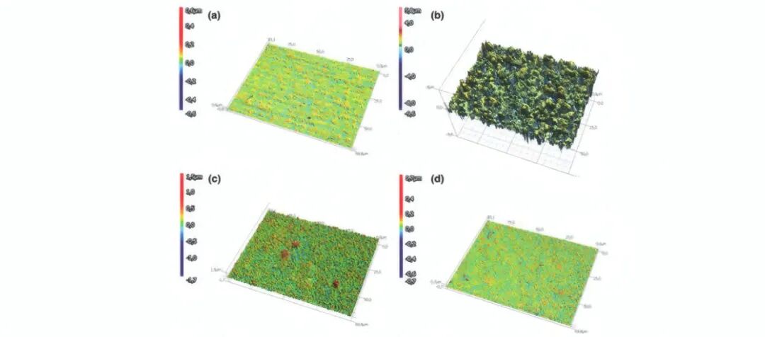
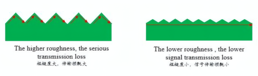
In PCB manufacturing, the width, thickness, and sidewall morphology of the traces directly affect the signal transmission characteristics and the current carrying capacity of the final product.Confocal microscopes can accurately measure the bottom width, top width, height, and sidewall angle, providing a comprehensive assessment of trace formation quality. Additionally, it can quantitatively analyze the surface roughness of copper foil, a parameter critical for signal transmission loss (especially in high-frequency applications) and the bonding strength of copper-clad laminates.
#Photonixbay.
Detection of Solder Mask Thickness and Coverage
The quality of the solder mask coating on PCBs is crucial for preventing circuit shorts and resisting environmental corrosion.Confocal microscopes can utilize their 3D imaging capabilities to accurately measure the thickness of the solder mask at different locations (such as on the trace surface and around pads), assessing its uniformity. At the same time, it can clearly reveal whether the solder mask completely covers the traces, and whether there are defects such as bridging, bubbles, or poor soldering, providing intuitive evidence for process optimization.
#Photonixbay.
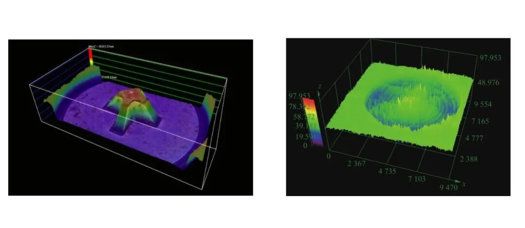
Quality Analysis of Microholes and Blind Holes
Uniformity of Electroplating in PCB Microholes
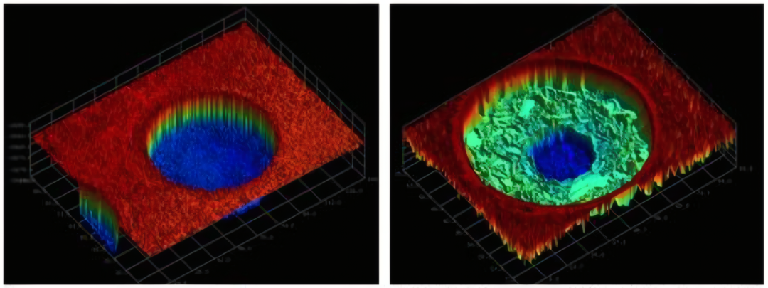
Microhole quality in high-density interconnect boards (HDI) is key to determining the reliability of inter-layer connections.Confocal microscopes can perform 3D reconstruction of microholes, accurately measuring the diameter, depth, wall roughness, and copper layer thickness at the hole entrance. This is crucial for assessing electroplating uniformity and identifying defects within the holes (such as voids and cracks), effectively preventing interconnection failures due to hole quality issues.
#Photonixbay.
Evaluation of Pads and Surface Treatment
Surface roughness and coating thickness of PCB pads directly affect the yield of component soldering.Confocal microscopes can non-destructively measure the thickness of coatings such as electroless nickel immersion gold (ENIG) and electroplated gold on pads, and can accurately characterize the micro-morphology at “black pad” defects caused by excessive corrosion, helping trace the root causes of process issues.
#Photonixbay.
Component Placement and Solder Joint Inspection
In the PCB assembly (SMT) stage, confocal microscopes can be used to measure the 3D shape, volume, and coplanarity of components after solder paste printing. For completed solder joints, it can clearly present the wetting angle, height, and surface morphology of the solder, assisting in the analysis of solder defects such as cold solder joints and shorts.
#Photonixbay.
Cleanliness and Contaminant Analysis
Contaminants on the surface of PCBs, such as fibers, dust, or chemical residues, can cause circuit leakage or corrosion.Confocal microscopes with high depth of field and resolution can quickly locate and identify these small contaminants, and combined with accessories such as energy dispersive spectroscopy (EDS), perform compositional analysis to guide improvements in cleaning processes.
#Photonixbay.
Advantages of Confocal Microscopes in the PCB Industry
-
Non-destructive acquisition of precise 3D data for key dimensions such as surface roughness and line width;
-
High-contrast imaging can clearly capture small scratches, contaminants, and other surface defects;
-
Compatible withvarious materials such as copper foil and solder mask, achieving clear imaging and precise measurement;
-
Non-contact measurement methods can avoid scratching soft or precision traces, ensuring sample integrity.
Confocal microscopes provide high-resolution 3D imaging, non-contact measurement, and excellent material adaptability, offering a comprehensive precision solution for the PCB industry from trace morphology, solder mask thickness, microhole quality, pad surface treatment, to solder joint inspection. In the face of trends towards high-density interconnection and new material applications, confocal technology has become a key tool for ensuring PCB product quality and driving process optimization.
#Photonixbay.
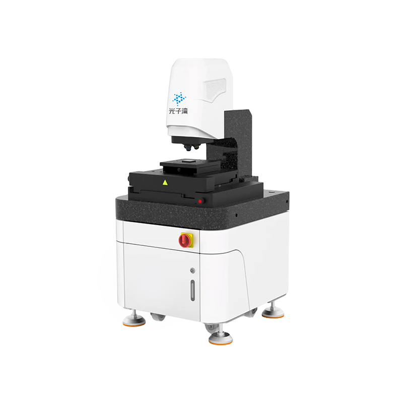
Photonixbay 3D Confocal Microscope
Photonixbay 3D Confocal Microscope is designed for the surface of various precision devices and materials, capable of handling diverse measurement scenarios, and can quickly and efficiently complete precision measurement tasks for sub-micron level morphology and surface roughness, providing reliable high-quality data.
Technical Support:199-6293-0018
-
Ultra-wide field of view, high-resolution color image observation
-
Provides roughness, geometric profile, structure, frequency, and functionality analysis techniques
-
Utilizes a pinhole confocal optical system with a high-stability structural design
-
Offers data processing capabilities for positioning, correction, filtering, and extraction across four major modules
Photonixbay Confocal Microscope provides characterization technology support for precision measurement with its in-situ observation and 3D imaging capabilities, aiding in the precise control of surface roughness and performance analysis, becoming an important optical measurement tool for driving technological upgrades across multiple fields.
#ConfocalMicroscope #ConfocalMicroscopeParameters #3DMicroscope #SurfaceRoughness #3DImaging
Thank you for reading. Photonixbay will continue to provide you with more high-quality content and progress together with you.
* Special Statement: The original and reprinted articles published by this public account are for academic sharing and conveying industry-related information only. Unauthorized acts such as plagiarism, alteration, citation, and reprinting that infringe upon the rights of this public account are prohibited. The content is for reference only; if there are copyright issues, please contact us, and we will verify and handle them promptly.
Previous Recommendations
Application of Confocal Microscopes in the OLED Panel Industry
Photonixbay Technology
Application of Confocal Microscopes in Polymer Material Research
Photonixbay Technology