▲ For more exciting content, please click on the blue text aboveand follow us!Typically, there are no dedicated courses in universities that teach the fundamentals of PCB grounding and decoupling; knowledge in this area often comes from laboratory experience or sharing from peers and seniors. Most electrical engineering graduates learn these skills on the job, so as long as everyone has a basic understanding of the key issues involved in the circuit design process (from schematic to layout to final PCB production), they will have a competitive advantage.
PCB Grounding Knowledge
1. Perfect Grounding vs. Imperfect GroundingFigure 1a shows a signal source separated from the load by a distance, with grounds G1 and G2 connected through a loop. Ideally, the grounding impedance between G1 and G2 is 0, so the ground loop current does not create a differential voltage between G1 and G2.
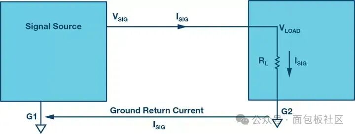
Figure 1a. At any point in the circuit, the arithmetic sum of currents is 0, meaning that whatever flows out must flow back. If the impedance between G1 and G2 is 0, then there is no differential voltage between G1 and G2.
Unfortunately, maintaining a zero-impedance return path is impossible; the grounding loop impedance will generate an error voltage ΔV between G1 and G2 under the influence of ground current. The connection between G1 and G2 has not only resistance but also inductance, ignoring the effects of stray capacitance. However, in the “Part 2: PCB Decoupling Knowledge” section of this article, we will learn how the capacitance between the power layer and the ground layer helps with high-frequency decoupling.
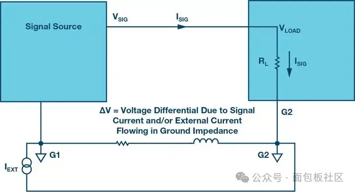
Figure 1b. The signal and/or external current flowing through the grounding impedance generates an error voltage ΔV.
The current flowing between G1 and G2 can be signal current or external current caused by other circuits.We can see how the total bus impedance in the test board shown in Figure 2 has both resistive and inductive components. Whether the grounding bus impedance affects circuit operation depends not only on the DC accuracy requirements of the circuit but also on the frequency of the analog signal and the frequency components generated by digital switching elements in the circuit.
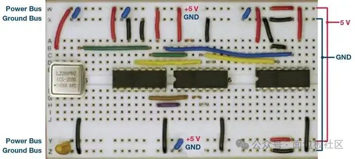
Figure 2. Circuit using a solderless test board.
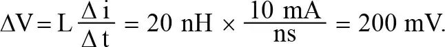
If the maximum signal frequency is 1 MHz and the circuit only requires a few milliamps (mA) of current, then the grounding bus impedance may not be an issue. However, if the signal is 100 MHz and the circuit drives a load requiring 100 mA, then the impedance is likely to become a problem.In most cases, using a “bus wire” as a digital grounding loop is unacceptable due to its impedance at most logic transition equivalent frequencies. For example, a #22 standard wire has about 20 nH/inch of inductance and 1 mΩ/inch of resistance. The transient current generated by logic signal transitions at a rate of 10 mA/ns flowing through 1 inch of this wire at this frequency will create a 200 mV useless voltage drop:
For a signal with a 2 V peak-to-peak range, this voltage drop translates to about a 10% error (approximately 3.5 bits of accuracy). Even in fully digital circuits, this error significantly reduces the logic noise margin. For low-frequency signals, this 1 mΩ/inch resistance also produces an error. For example, when a 100 mA current flows through 1 inch of #22 standard wire, the resulting voltage drop is approximately:

A signal with a 2 V peak-to-peak range digitized to 16-bit accuracy has 1 LSB = 2 V/216 = 30.5 μV. Therefore, the 100 μV error caused by wire resistance is approximately equal to a 3.3 LSB error at the 16-bit accuracy level. Figure 3 shows how high noise digital currents flowing in the analog grounding loop generate errors in the input voltage VIN of the analog circuit. Connecting the analog circuit ground and digital circuit ground at the same point (as shown in the correct circuit diagram below) can mitigate the above issues to some extent.
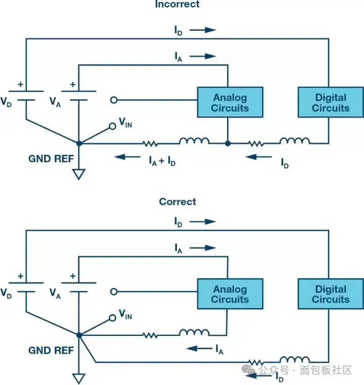
Figure 3. Using a single-point ground for analog and digital circuits can reduce the error effects caused by high noise digital circuits.
2. Ground Layers are Essential in Today’s SystemsIn solderless test boards, and even in circuit boards using a bus structure as shown in Figure 2, there are not many means available to reduce grounding impedance. Solderless test boards are very rare in industrial system design. A solid ground layer is the industrial standard method for providing a low-impedance return path. Production printed circuit boards generally have one or more layers specifically for grounding. This method is quite suitable for final production but is difficult to implement in prototype systems.Figure 4 shows a typical grounding arrangement for a PCB containing analog circuits, digital circuits, and a mixed-signal device (such as an ADC or DAC).
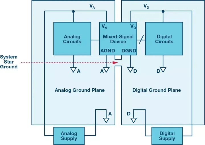
Figure 4. Good grounding solutions for mixed-signal system PCBs.
Analog circuits and digital circuits are physically isolated, each located on their respective ground layers. Mixed-signal devices span both ground layers, with the system’s single-point or star grounding being the connection point between the two ground layers.We have learned that there are other proven grounding principles regarding analog and digital grounding, all based on the same concept—analyzing the paths of analog and digital currents and then taking measures to minimize their mutual interference.
PCB Decoupling Knowledge
1. Understand Decoupling Requirements Based on Power Supply Rejection ParametersAnalog integrated circuits such as amplifiers and converters have at least two or more power pins. For single-supply devices, one pin is typically connected to ground, while mixed-signal devices like ADCs and DACs can have analog and digital power voltages as well as I/O voltages. Digital ICs like FPGAs can also have multiple power voltages, such as core voltage, memory voltage, and I/O voltage.No matter how many power pins there are, the IC datasheet specifies the allowable range for each power supply, including recommended operating ranges and maximum absolute values, and these limits must be adhered to for normal operation and to prevent damage. However, even slight variations in power supply voltage due to noise or power supply ripple—even if still within the recommended operating range—can lead to degraded device performance. For example, in an amplifier, slight changes in power supply can produce small variations in input and output voltages, as shown in Figure 5.
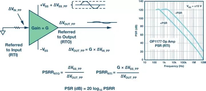
Figure 5. Power supply rejection shows the sensitivity of output voltage to changes in power supply rails.
The sensitivity of amplifiers to changes in power supply voltage is typically quantified by the Power Supply Rejection Ratio (PSRR), defined as the ratio of the change in power supply voltage to the change in output voltage. Figure 5 shows the PSR of a typical high-performance amplifier (OP1177) decreasing at approximately 6 dB/8 octaves (20 dB/10 octaves) with frequency, with curves shown for both positive and negative power supplies. Although the PSRR is 120 dB at DC, it decreases rapidly at higher frequencies, at which point more and more useless energy on the power line couples directly to the output.If the amplifier is driving a load and there is useless impedance on the power rails, the load current will modulate the power rails, increasing noise and distortion in the AC signal.Although the actual PSRR may not be provided in the datasheet, the performance of data converters and other mixed-signal ICs will also degrade with noise on the power supply. Power supply noise can affect digital circuits in various ways, including reducing the noise margin of logic levels and causing timing errors due to clock jitter.2. Proper Local Decoupling is Essential on PCBsA typical 4-layer PCB is usually designed with a ground layer, power layer, top signal layer, and bottom signal layer. The ground pins of surface-mount ICs are directly connected to the ground layer through vias, minimizing useless impedance in the ground connection.Power rails are typically located on the power layer and routed to various power pins of the IC. A simple IC model showing power and ground connections is shown in Figure 6.
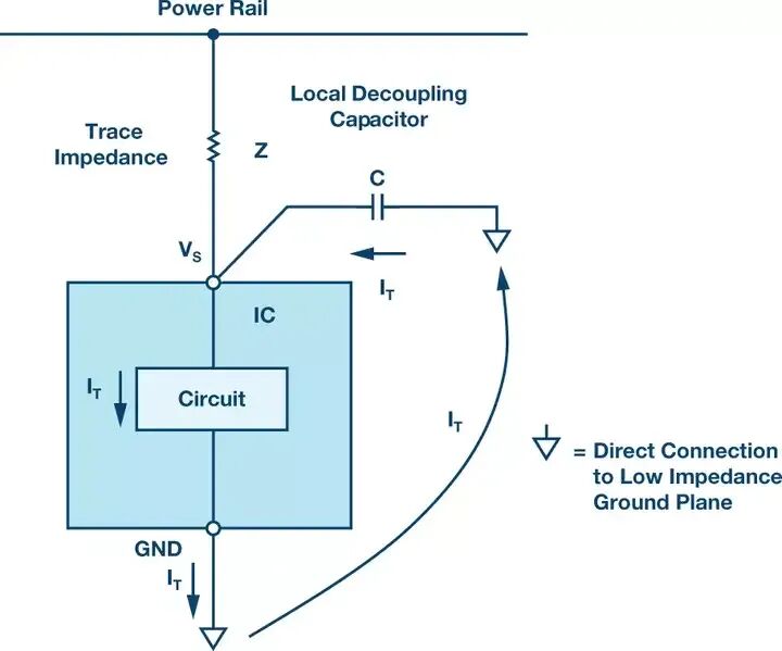
Figure 6. IC model showing trace impedance and local decoupling capacitors.
The current generated within the IC is represented as IT. The current flowing through the trace impedance Z causes a change in the power supply voltage VS. As mentioned above, this will result in various types of performance degradation depending on the IC’s PSR.By using the shortest possible connections, appropriate types of local decoupling capacitors can be directly connected between the power pins and the ground layer, minimizing sensitivity to power noise and ripple. Decoupling capacitors act as charge reservoirs for transient currents and shunt them directly to ground, maintaining a constant power supply voltage across the IC. Although the return current path goes through the ground layer, the low impedance of the ground layer generally does not produce significant error voltage.Figure 7 shows that high-frequency decoupling capacitors must be placed as close to the chip as possible. Otherwise, the inductance of the connecting traces will adversely affect the effectiveness of the decoupling.
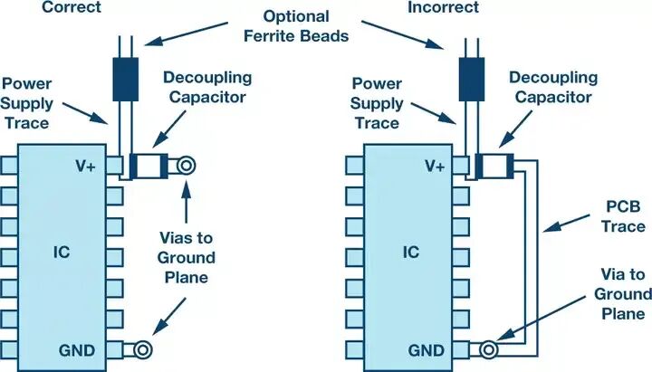
Figure 7. Correct and incorrect placement of high-frequency decoupling capacitors.
On the left side of Figure 7, both the power pin and ground connection can be short, making it an effective configuration. However, on the right side of Figure 7, the additional inductance and resistance within the PCB traces will reduce the effectiveness of the decoupling scheme, and increasing the closed loop may cause interference issues.3. Choosing the Right Type of Decoupling CapacitorLow-frequency noise decoupling typically requires electrolytic capacitors (typical values range from 1μF to 100μF) to serve as charge reservoirs for low-frequency transient currents. Low-inductance surface-mount ceramic capacitors (typical values range from 0.01μF to 0.1μF) should be directly connected to the IC power pins to effectively suppress high-frequency power noise. All decoupling capacitors must be directly connected to a low-inductance ground layer to be effective. This connection requires short traces or vias to minimize additional series inductance.Most IC datasheets provide recommended power decoupling circuits in the application section, and these recommendations should always be followed to ensure proper device operation.Ferrite beads (made from insulating ceramics of nickel, zinc, manganese oxides, or other compounds) can also be used for decoupling in power filters. Ferrites are inductive at low frequencies (<100kHz)—thus useful for low-pass LC decoupling filters. Above 100kHz, ferrites become resistive (low Q). The impedance of ferrites is a function of material, operating frequency range, DC bias current, number of turns, size, shape, and temperature.Ferrite beads are not always necessary but can enhance high-frequency noise isolation and decoupling, often being beneficial. It is important to verify that the ferrite does not saturate, especially when operational amplifiers drive high output currents. When ferrites saturate, they become nonlinear and lose filtering characteristics. It is crucial to note that some ferrites may even be nonlinear before fully saturating, so if a power stage is required to operate with low distortion output, ferrites should be checked when prototypes operate near this saturation region. Typical ferrite bead impedance is shown in Figure 8. When selecting the appropriate type for decoupling applications, careful consideration must be given to the non-ideal capacitive performance due to parasitic resistance and inductance.
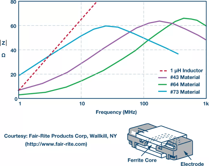
Figure 8. Impedance of ferrite beads.
PCBs are the support for electronic components and the carrier for electrical connections between them, often referred to as “electronic aircraft carriers” and widely used in communications, consumer electronics, computers, and more. Designing an excellent PCB is no easy task. At the same time, PCB design is the foundation of hardware circuit design and is essential for electronic engineers; solidifying the foundation is crucial for building high structures.Click to read the original text and unlock the opportunity for in-depth discussions with industry veteran engineers.Source: ADI
· END ·
Welcome to follow the subscription account of EEWorld: "Automotive Development Circle"

Scan to add the assistant and reply “Join Group”
to exchange experiences face-to-face with electronic engineers.