“Personal reading notes, for learning and communication purposes only”
Introduction
Due to the rising price of gold, the existing ENIG surface treatment process is facing price pressure. Therefore, a comparison of the advantages and disadvantages of different surface treatment processes has been organized.
PCB surface treatment technology refers to the process of artificially forming a layer on the PCB components and electrical connection points that has different mechanical, physical, and chemical properties from the substrate. The purpose is to ensure good solderability or electrical performance of the PCB. Since copper tends to exist in the form of oxides in the air, which severely affects the solderability and electrical performance of the PCB, surface treatment is necessary. Currently, common surface treatment processes include HASL (Hot Air Solder Leveling), ENIG (Electroless Nickel Immersion Gold), OSP (Organic Solderability Preservative), ImSn (Immersion Tin), ImAg (Immersion Silver), ENEPIG (Electroless Nickel Electroless Palladium Immersion Gold), etc. Each process has different characteristics, such as cost, solderability, and environmental friendliness.
01
Hot Air Solder Leveling
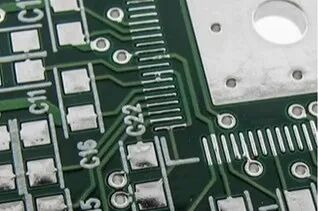
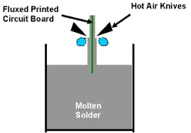
HASL (Hot Air Solder Leveling) is the process of immersing the PCB in molten solder (traditional leaded or lead-free solder), and then using strong hot air to blow away the excess solder and level the surface, forming a layer that resists copper oxidation (2~40um), providing a good solderable coating.
Advantages:
- Currently the most common and cheapest method;
- Thick solder layer, good solderability, wide soldering window, long storage time;
- Provides good mechanical strength for solder joints.
Disadvantages:
- Surface is uneven, not suitable for fine-pitch components (such as BGA, QFN);
- High-temperature process (especially lead-free HASL) may cause thermal shock to the substrate;
- Solder composition may cover vias, leading to subsequent soldering issues;
- Lead-containing HASL does not meet RoHS and other environmental requirements (lead-free HASL is mainstream).
- Not suitable for double-sided mounting, secondary reflow may cause copper-tin compounds leading to poor soldering.
Applicable scenarios: Consumer electronics, industrial control boards, applications sensitive to cost and with not particularly fine component spacing.
02
Electroless Nickel Immersion Gold
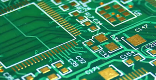
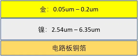
First, a layer of nickel (2.54~6.35um) is chemically deposited on the copper pads as a barrier and soldering layer, and then a thin layer of gold (0.05~0.2um) is deposited through a displacement reaction to protect the nickel layer from oxidation. Reference standard IPC-4552A
Advantages:
- Surface is very flat, ideal for fine-pitch components (BGA, 0603/0402 resistors and capacitors, QFP, etc.);
- Gold layer has excellent oxidation resistance, good solderability, and long-term storage stability (usually >12 months);
- Nickel layer provides good solder joint strength and diffusion barrier;
- Suitable for wire bonding;
- Meets RoHS requirements.
Disadvantages:
- Relatively high cost (second only to ENEPiG);
- Risk of “black pad”: Nickel is highly active and turns black after oxidation;
- Thin gold layer quickly dissolves into solder after soldering, making the solder joint actually a connection between solder and nickel.
- Nickel has high-speed signal loss, not suitable for high-speed boards.
Applicable scenarios: Smartphones, tablets, server motherboards, networking devices, high-end consumer electronics, medical devices, etc., high-density interconnect boards that require good bonding performance.
03
Immersion Silver
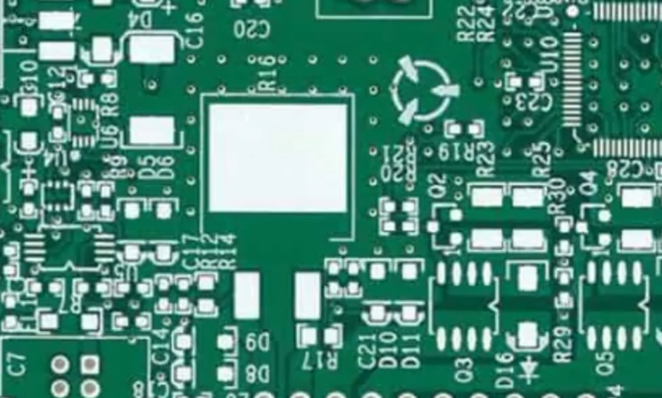
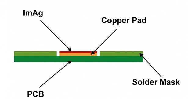
Depositing a thin layer of silver (0.1~0.3um) on the copper pads through a displacement reaction. Standard reference IPC-4553A.
Advantages:
- The process is between OSP and electroless nickel, relatively simple and fast;
- Surface is very flat, suitable for fine-pitch components;
- Excellent solderability, soldering performance close to bare copper;
- Good high-frequency signal transmission performance (Ag has low skin effect loss);
- Cost is between HASL and ENIG;
- Meets RoHS requirements.
Disadvantages:
- Silver layer is prone to oxidation and sulfide (exposed to sulfur-containing environments will turn yellow and black), affecting solderability and appearance (requires sulfur inhibitors and strict packaging);
- Storage life is shorter than ENIG (usually 6–12 months), requires inert gas packaging;
- Risk of microvoids (high process control requirements);
- Risk of electrochemical migration (silver migration) in humid environments, dendrite issues.
Applicable scenarios: High-speed digital and high-frequency analog circuit boards (such as RF, antennas), LED lighting, automotive electronics (with attention to sulfide issues), applications with extremely high soldering performance requirements.
04
Immersion Tin
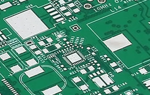
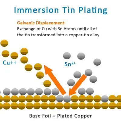
Depositing a thin layer of tin (1.15-1.3um) on the copper pads through a chemical displacement reaction. Standard reference IPC-4554.
Advantages:
- Flat surface, suitable for fine-pitch components;
- Tin has good compatibility with solder, can match any type of solder, excellent solderability;
- Suitable for press-fit connections;
- Cost is between HASL and OSP;
- Immersion tin process can form flat copper-tin intermetallic compounds, which gives immersion tin good solderability similar to hot air leveling.
- Meets RoHS requirements.
Disadvantages:
- Tin layer is prone to whiskers, especially under high temperature, high humidity, or stress (can be suppressed by adding organic additives, but risks still exist);
- Storage life is shorter than ENIG (usually around 6 months), requires attention to storage conditions;
- Tin layer is relatively soft and easily scratched;
- Repeated reflow soldering may consume the tin layer, potentially leading to decreased solderability.
Applicable scenarios: Automotive electronics (need to pay attention to whisker risk control), applications requiring press-fit connections, applications that require flatness and are cost-sensitive.
05
Organic Solderability Preservative (OSP)
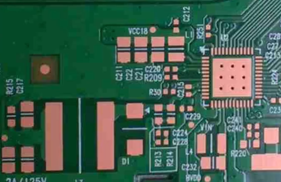
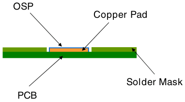
OSP is a water-soluble organic compound coated on clean copper pads by chemical means (reference standard IPC-4555), forming a very thin organic protective film (0.2-0.6um) to prevent copper oxidation. This protective film will evaporate during high-temperature soldering, ensuring effective soldering between solder and copper foil. Common organic films include ENTEC106.
Advantages:
- Low cost, even lower than soldering;
- Flat surface, suitable for fine-pitch components;
- Simple process, environmentally friendly (no heavy metals);
- The protective film has anti-oxidation, thermal shock resistance, and moisture resistance, preventing the copper surface from continuing to rust (oxidation or sulfide, etc.) in normal environments;
- The solder joint is actually a direct connection between solder and copper, which can be quickly removed by flux during subsequent high-temperature soldering, ensuring high reliability.
Disadvantages:
- The protective film is thin and fragile, easily scratched;
- Not point-to-point, thus not suitable for ICT testing;
- Relatively short storage life (usually 3-6 months), requires strict packaging and storage (low humidity, light avoidance);
- Solderability is limited by multiple reflow soldering (the protective film decomposes at high temperatures);
- The protective film needs to be removed before soldering (dissolved under the action of flux), which requires high soldering process requirements;
- Thickness is not easy to detect and measure;
- Not suitable for wire bonding.
Applicable scenarios: Cost-sensitive consumer electronics that require flat surfaces, computer motherboards, communication boards, products with high-volume production and fast turnover.
06
Electroplated Nickel Gold
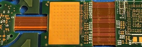
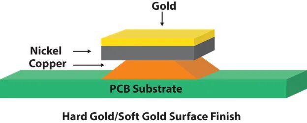
Electroplated nickel gold is divided into “hard gold” and “soft gold.” Hard gold has a lower purity (99.6%) and is commonly used for gold fingers (PCB edge connectors), PCB contacts, or other hard-wearing areas. The thickness of gold can vary according to requirements. Soft gold is purer (99.9%) and is usually used for wire bonding.
Advantages:
-
Can be used for wire bonding: thicker gold layers are suitable for wire bonding.
-
Extremely high wear resistance: The gold layer is hard and wear-resistant, making it very suitable for connectors (gold fingers) and contact points that require frequent plugging and unplugging.
-
Excellent conductivity: Gold has excellent conductivity, providing reliable electrical contact.
Disadvantages:
-
Very high cost: The process is complex, and the thickness of the gold layer is much higher than that of immersion gold, leading to high costs.
-
Poor solderability: The gold plating layer is usually thick, making it easy to form brittle gold-tin compounds during soldering, affecting solder joint strength and reliability. Therefore, it is usually not used in soldering areas.
-
Requires jumpers/conductive rods: Additional jumpers or conductive rods are needed for electroplating.
Applicable scenarios: Mainly used for PCB edge connectors (gold fingers), keyboard contact points, test probes, etc., in areas requiring high wear resistance and reliable electrical contact.
07
Electroless Nickel Palladium Gold
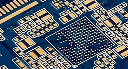
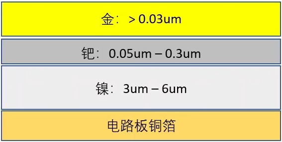
Electroless nickel palladium gold has an additional layer of palladium between nickel and gold compared to electroless nickel immersion gold, which can prevent corrosion caused by displacement reactions, preparing for the immersion gold. Gold tightly covers the palladium, providing a good contact surface. Reference standard IPC-4556.
Advantages:
- Compared to ENIG, ENEPIG has an additional palladium layer between nickel and gold, further protecting the nickel layer from corrosion and overcoming the “black pad” issue of ENIG (the palladium layer prevents nickel corrosion);
- Extremely flat surface, suitable for ultra-fine pitch components and advanced packaging;
- Extremely long storage life;
- Extremely excellent solderability;
- Perfectly supports both soldering and wire/aluminum bonding;
- Palladium layer is an excellent diffusion barrier.
- Compensates for nickel’s high-speed signal loss, suitable for high-frequency applications.
Disadvantages:
- Highest cost (palladium is a precious metal);
- Complex process, high control requirements.
Applicable scenarios: High-end servers, core communication devices, aerospace, military electronics, applications requiring extremely high reliability and supporting both soldering and bonding, chip-level packaging.
08
Selection Logic
- Cost priority, general applications: HASL (lead-free) or OSP.
- High density, high reliability, long storage: ENIG (mainstream choice).
- High-speed/high-frequency signals: IAg (with attention to sulfide protection).
- Cost-sensitive and requiring flatness, fast turnover: OSP or ISn (watch for whiskers).
- Top-end, requiring bonding and soldering, extreme reliability: ENEPIG (regardless of cost).
- Soldering times: OSP surface treatment process is not suitable for more than two reflows.
In practical applications, ENIG has become the mainstream and most widely used surface treatment process due to its excellent overall performance (flatness, solderability, reliability, storability) and relatively reasonable cost. Engineers should make the most suitable choice based on the specific needs and constraints of the product.