1. Considerations for Component Packaging in RF Circuits
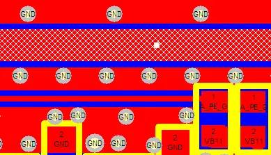
A successful RF design must pay careful attention to every step and detail throughout the design process, which means thorough and careful planning must be done from the start of the design phase, along with comprehensive and continuous evaluation of the progress of each design step. This meticulous design skill is something that most electronic companies in China lack.In recent years, the demand and growth for Bluetooth devices, wireless local area network (WLAN) devices, and mobile phones have prompted practitioners to pay more attention to the skills of RF circuit design. From the past to the present, RF circuit board design has been one of the most challenging aspects for engineers, akin to electromagnetic interference (EMI) issues, and even a nightmare. To achieve success in design in one go, careful planning and attention to detail are essential.RF circuit board design is often described as a “black art” due to the many uncertainties it involves theoretically. However, this is just a one-sided view; there are many rules to follow in RF circuit board design. However, the truly practical skills in actual design lie in how to compromise these rules when various constraints prevent their implementation. Important RF design topics include: impedance and impedance matching, insulation layer materials and stack-up, wavelength and harmonics, etc.In the development process of WiFi products, the layout of RF circuits (RF Circuit Layout Guide) is an extremely critical process. Many times, we may have designed very well in principle, but after the actual board production, the results are not ideal; in reality, these are all due to insufficient perfection in the layout. This article will explain some issues that should be noted in RF circuit layout using an example of a wireless network card layout and some of my work experiences.PCB Stack-UpBefore proceeding with layout, we must first determine the stack-up of the circuit board, just like building a house requires walls first. The determination of the stack-up of the circuit board relates to many factors such as the complexity of the circuit design and considerations for electromagnetic compatibility. The diagram below shows common stack-up configurations for four-layer, six-layer, and eight-layer boards.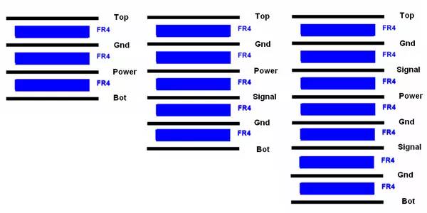 In the PCB stack-up of wireless network cards, single-sided boards generally do not occur, so this article will not discuss single-sided boards.Considerations for two-layer board design.In the design of four-layer boards, we generally use the second layer as a complete ground plane, while also routing important signal lines on the top layer (including RF traces) to facilitate good impedance control. In six-layer boards or more complex designs, we will similarly use the second layer as a complete ground plane, while routing the most important signal lines on the top layer.PS: You can use Polar to calculate single-ended impedance and other impedances; some layout software has built-in impedance calculators, such as Allegro.Impedance ControlAfter we perform schematic design and simulation, one thing worth noting in layout is impedance control. As we all know, we should try to ensure that the characteristic impedance of the traces is 50 ohms, which mainly relates to trace width. In this example, it is two and a half layers, and in Polar, using the Surface Coplanar Line model for impedance calculation, we can obtain a set of relatively ideal values: Height (H) = 39.6 mil, Track (W) = 30 mil, Track (W1) = 30 mil, Thickness = 1 OZ = 1.4 mil, Separation (S) = 7 mil, Dielectric (Er) = 4.2, resulting in a characteristic impedance of 52.14 ohms, which meets the requirements. The highlighted trace in the diagram below is such an RF trace.
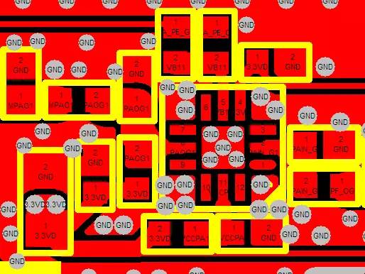
 Placement of RF ComponentsThose who have done RF design should know that we should keep the trace lengths as short as possible, and the placement of components should be as compact as possible (except for special requirements), while also ensuring that the placement of components is favorable for routing (to avoid routing traces in a convoluted manner). In the diagram below, we see the placement of components around an RF power amplifier (PA, Power Amplifier), where the distance between components is minimal.
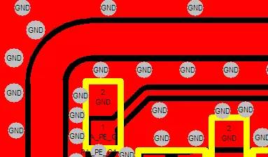
 Considerations for RF TracesAs mentioned earlier, the lengths of RF traces should be kept as short as possible, and the trace widths should be set strictly according to the calculated values. It is especially important that there are no sharp bends in RF traces; at the corners, it is best to use curves to achieve this, as shown in the diagram below.
 Secondly, in multi-layer board routing, important RF lines may inevitably cross; in this case, we will have to use the last thing we want to use: vias. This means that some RF signal lines will run to the bottom layer or even to the middle layer, but regardless of which layer, RF traces must have a reference plane. A noteworthy issue here is to avoid crossing layers or making the ground plane discontinuous.Placement of ViasThe placement of vias is indeed a complex matter; this article will only discuss grounding vias.First, the ground line next to the RF trace should ideally penetrate through vias to connect to the bottom layer or the ground plane in the middle layer, as this provides the shortest path for any interference signals or radiation to reach the ground. However, the vias cannot be too close to the RF signal lines, or it will severely affect the quality of the RF signal. In actual design, this can be flexibly handled; as shown in the diagram below, we see many vias distributed across the highlighted signal line.
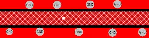 Secondly, in areas with large ground planes, we usually place many vias to connect the grounds of different layers. In RF circuit routing, it is important that large vias are placed irregularly to maximize the suppression of various interferences.2. Considerations for Power Supply Design in RF Circuits(1) The power supply line is an important pathway for EMI to enter and exit the circuit. Through the power supply line, external interference can enter the internal circuit, affecting RF circuit indicators. To reduce electromagnetic radiation and coupling, it is required that the loop area on the primary side, secondary side, and load side of the DC-DC module be minimized. Regardless of how complex the power supply circuit is, its large current loop should be kept as small as possible. The power supply line and ground line should always be placed close to each other.(2) If a switching power supply is used in the circuit, the layout of peripheral components of the switching power supply should comply with the principle of the shortest possible power return path. The filtering capacitors should be placed close to the relevant pins of the switching power supply. Common mode inductors should be placed near the switching power supply module.(3) Long-distance power supply lines on the same board should not be close to or cross near the output and input terminals of cascaded amplifiers (gain greater than 45dB). This is to avoid the power supply line becoming a transmission path for RF signals, which may cause self-excitation or reduce sector isolation. High-frequency filtering capacitors should be added at both ends of long-distance power supply lines, and even in the middle.(4) At the power supply entrance of RF PCBs, three filtering capacitors should be combined in parallel, utilizing the advantages of each of these capacitors to filter out low, medium, and high frequencies on the power supply line. For example: 10uF, 0.1uF, 100pF, and arranged in order from largest to smallest, closest to the input pin of the power supply.(5) When using the same group of power supplies to power small signal cascaded amplifiers, the supply should start from the last stage and proceed to the front stage, to minimize the impact of EMI generated by the last stage circuit on the preceding stage. Each stage’s power supply filtering should have at least two capacitors: 0.1uF and 100pF. When the signal frequency exceeds 1GHz, a 10pF filtering capacitor should be added.(6) Commonly used low-power electronic filters should have filtering capacitors placed close to transistor pins, with high-frequency filtering capacitors even closer to the pins. Transistors should be selected with a lower cutoff frequency. If the transistors in the electronic filter are high-frequency devices operating in the amplification region, and the layout of peripheral components is not reasonable, high-frequency oscillation can easily occur at the power output end. Linear voltage regulator modules may also have similar issues due to feedback loops present in the chip, with internal transistors working in the amplification region. During layout, high-frequency filtering capacitors should be placed close to the pins to reduce distributed inductance and disrupt oscillation conditions.(7) The copper foil size of the POWER section of the PCB should meet the maximum current flowing through it, considering a margin (generally referenced as 1A/mm width).(8) The input and output of the power supply lines should not cross.(9) Pay attention to power supply decoupling and filtering to prevent different units from generating interference through the power supply line; during power supply routing, the power supply lines should be isolated from each other. The power supply line should be isolated from other strong interference lines (such as CLK) using ground lines.(10) The power supply routing of small signal amplifiers needs to be isolated with ground copper foil and grounding vias to prevent other EMI interference from entering and deteriorating the signal quality of this stage.(11) Different power supply layers should avoid overlapping in space. This is mainly to reduce interference between different power supplies, especially between power supplies with significant voltage differences; the overlapping issue of power planes should be avoided as much as possible, and if unavoidable, consider using an intermediate ground layer.(12) The layer allocation of PCBs should simplify subsequent routing processes. For a four-layer PCB (commonly used in WLAN), in most applications, components and RF leads should be placed on the top layer, the second layer should serve as the system ground, the power section should be placed on the third layer, and any signal lines can be distributed on the fourth layer.The use of a continuous ground plane layout on the second layer is essential for establishing impedance-controlled RF signal paths, and it also facilitates obtaining the shortest possible ground loop, providing high electrical isolation between the first and third layers, minimizing coupling between the two layers. Of course, other board layer definitions can be adopted (especially when the circuit board has different numbers of layers), but the above structure is a validated successful example.
 (13) Large-area power layers can make Vcc routing easier, but this structure often triggers a deterioration in system performance. Connecting all power leads together on a larger plane will inevitably lead to noise transmission between pins. Conversely, using a star topology can reduce coupling between different power pins.
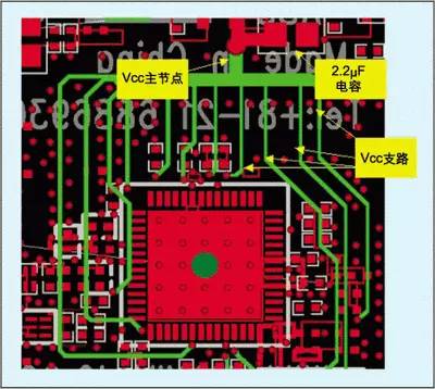 The diagram above shows a star-connected Vcc routing scheme, extracted from the evaluation board of the MAX2826 IEEE 802.11a/g transceiver. The diagram establishes a main Vcc node, from which different branches of power lines extend to supply power to the RF IC’s power pins. Each power pin uses independent leads to provide spatial isolation between the pins, which is beneficial for reducing coupling between them. Additionally, each lead also has a certain amount of parasitic inductance, which is precisely what we want, as it helps filter out high-frequency noise on the power supply line.When using star topology Vcc leads, it is also necessary to take appropriate power supply decoupling measures, as decoupling capacitors have a certain amount of parasitic inductance. In fact, capacitors are equivalent to a series RLC circuit; the capacitor dominates at low frequencies, but at self-excited oscillation frequencies (SRF):
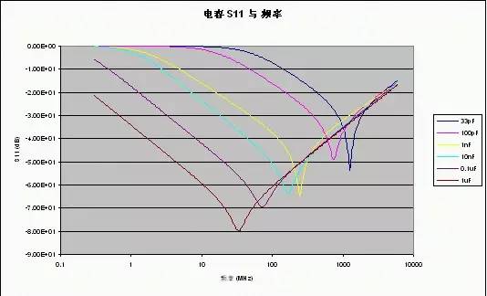
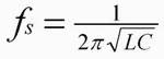 The impedance of the capacitor will become inductive. Thus, it can be seen that capacitors only have decoupling effects at frequencies close to or below their SRF; at these frequency points, the capacitor exhibits low resistance.Typical S11 parameters under different capacitance values are shown; from these curves, it can be clearly seen that the SRF appears, and it can also be observed that the larger the capacitance, the better the decoupling performance provided at lower frequencies (the exhibited impedance is lower).At the main node of the Vcc star topology, it is best to place a large-capacity capacitor, such as 2.2μF. This capacitor has a lower SRF and is effective at eliminating low-frequency noise and establishing stable DC voltage. Each power pin of the IC requires a low-capacity capacitor (such as 10nF) to filter out high-frequency noise that may couple onto the power supply line. For power pins supplying noise-sensitive circuits, it may be necessary to externally connect two bypass capacitors. For example, a 10pF capacitor in parallel with a 10nF capacitor can provide bypassing across a wider frequency range, minimizing the noise impact on the power supply voltage. Each power pin should be carefully examined to determine the necessary decoupling capacitance and which frequency points in the actual circuit are susceptible to noise interference.Good power supply decoupling techniques, combined with rigorous PCB layout and Vcc leads (star topology), can lay a solid foundation for any RF system design. Although other factors may still exist in actual design that can reduce system performance metrics, having a “noise-free” power supply is a fundamental element in optimizing system performance.3. EMC Specifications for RF PCB Design1 Layer Distribution1.1 For double-sided boards, the top layer is the signal layer, and the bottom layer is the ground plane.1.2 For four-layer boards, the top layer is the signal layer, the second layer is the ground plane, and the third layer carries power and control lines. In special cases (such as when RF signal lines need to pass through shielding walls), some RF signal lines should be routed on the third layer. Each layer requires a large area of grounding.1.2 For four-layer boards, the top layer is the signal layer, the second layer is the ground plane, and the third layer carries power and control lines. In special cases (such as when RF signal lines need to pass through shielding walls), some RF signal lines should be routed on the third layer. Each layer requires a large area of grounding.2 Grounding2.1 Large-area grounding is recommended to reduce the impedance of the ground plane and achieve good grounding effects. The following requirements should be adhered to: a) RF PCB grounding requires large area grounding; b) In microstrip printed circuits, the bottom surface must be a ground plane and must be smooth and flat; c) The contact surface of the ground should be gold-plated or silver-plated for good conductivity to reduce ground resistance; d) Use fastening screws to tightly bind it to the shielding cavity, with a screw spacing of less than λ/20 (depending on the specific situation).2.2 Grouped nearby grounding: The entire circuit should be divided into relatively independent groups based on the circuit structure and current size, with each group grounded nearby to form a loop. The direction of high-frequency filtering capacitors within each group should be adjusted to minimize the power loop. Note that grounding lines should be short and straight, and crossing or overlapping should be avoided to reduce interference caused by common ground impedance.2.3 Grounding of RF components: Surface-mounted RF components and filtering capacitors that require grounding should minimize the grounding inductance of the components: a) At least two lines should connect to the grounding copper foil; b) At least two metallized vias should be placed near the component pins for grounding; c) Increase the via diameter and parallel several vias; d) Some components have metal shells grounded at the bottom; grounding holes should be added within the projection area of the components, and no signal lines should be routed on the surface layer.2.4 Grounding of microstrip circuits: The terminal single grounding vias must be larger than the microstrip line width, or use a large number of small holes densely arranged for grounding.2.5 Grounding process requirements: a) To the extent allowed by the process, the distance between pads and vias can be shortened; b) To the extent allowed by the process, large grounding pads can be directly covered by at least 6 grounding vias (the specific number depends on the pad size); c) When grounding lines need to travel a certain distance, their lengths should be shortened, and should not exceed λ/20 to prevent antenna effects from causing signal radiation; d) Except for special purposes, isolated copper foil should not exist, and grounding vias must be added to copper foil; e) No ends of open lines should extend from the grounding copper foil.3 Shielding3.1 RF signals can radiate in air media. The larger the spatial distance, the lower the operating frequency, the smaller the parasitic coupling at the input and output ends, and the greater the isolation. The typical spatial isolation of PCBs is about 50dB.3.2 Sensitive circuits and strong radiation source circuits should be shielded, but if design and processing are difficult (due to spatial or cost limitations, etc.), shielding can be omitted, but tests should be conducted to make a final decision. These circuits include:a) The front end of the receiving circuit is a sensitive circuit with a very weak signal, requiring shielding.b) RF units and intermediate frequency units must be shielded. Intermediate frequency signals in the receiving channel can greatly interfere with RF signals, and conversely, RF signals in the transmitting channel can also cause radiation interference to intermediate frequency signals.c) Oscillator circuits: strong radiation sources should be shielded separately from the local oscillator source, as the local oscillator level is relatively high and can cause significant radiation interference to other units.d) Power amplifiers and antenna feed circuits: strong radiation sources with strong signals require shielding.e) Digital signal processing circuits: strong radiation sources; the steep edges of high-speed digital signals can interfere with analog RF signals.f) Cascaded amplifier circuits: the total gain may exceed the spatial isolation from output to input, satisfying one of the conditions for oscillation; the circuit may self-excite. If the gain of the circuit within the cavity exceeds 30-50dB, a metal shielding plate must be soldered or installed on the PCB to increase isolation. In actual design, frequency, power, and gain conditions should be comprehensively considered to decide whether to add a shielding plate.g) Cascaded filtering, switching, and attenuation circuits: within the same shielding cavity, the out-of-band attenuation of cascaded filtering circuits, the isolation of cascaded switching circuits, and the attenuation of cascaded attenuation circuits must be less than 30-50dB. If this value is exceeded, a metal shielding plate must be soldered or installed on the PCB to increase isolation. In actual design, frequency, power, and gain conditions should be comprehensively considered to decide whether to add a shielding plate.h) Transceiver units should be shielded when mixed.i) When mixing digital and analog circuits, the clock lines should be isolated or shielded with grounding copper foil.4 Shielding Materials and Methods4.1 Commonly used shielding materials are high-conductivity materials, such as copper plates, copper foils, aluminum plates, and aluminum foils. Steel plates or metal coatings, conductive coatings, etc.4.2 Electrostatic shielding is mainly used to prevent the effects of electrostatic fields and constant magnetic fields. Two basic points should be noted: a complete shielding body and good grounding.4.3 Electromagnetic shielding is mainly used to prevent the effects of alternating magnetic fields or alternating electromagnetic fields, requiring the shielding body to have good conductive continuity, and the shielding body must connect to a common ground reference plane with the circuit, requiring the shielding ground in the PCB to be as close as possible to the ground of the shielded circuit.4.4 For some sensitive circuits, circuits with strong radiation sources can design a soldered shielding cavity on the PCB; during design, “via shielding walls” should be added, which are grounding vias at the locations on the PCB that are in close contact with the walls of the shielding cavity. The requirements are as follows:a) There should be more than two rows of vias;b) Two rows of vias should be staggered;c) The spacing of vias in the same row should be less than λ/20;d) The PCB copper foil that contacts the shielding cavity wall should not have solder mask.4.5 When RF signal lines pass through shielding walls on the top layer, a slot should be opened at the corresponding position of the shielding cavity, with a height greater than 0.5mm and a width ensuring that the distance between the signal line and the shielding body after installing the shielding wall is greater than 1mm.5 Shielding Cover Design5.1 Basic structure of metal shielding cavities5.1.1 Such shielding covers are widely used, as shown in Figure 27. The material is generally thin aluminum alloy, and the manufacturing process typically involves stamping, bending, or pressure casting. These shielding covers have many screw holes for easy fixing with screws. Some require aluminum alloy covers and absorbing materials to enhance shielding performance. RF PCBs must be housed within shielding cavities, and appropriate sizes for shielding cavities should be chosen to ensure that their lowest resonant frequency is far above the operating frequency, ideally more than 10 times higher; see Appendix G “Design of Metal Shielding Cavities” for details.5.1.2 The height of the shielding cavity is generally 15-20 times or more than the thickness of the first dielectric. When the area of the shielding cavity is fixed, to increase the lowest resonant frequency of the shielding cavity, the aspect ratio should be increased, avoiding square cavities, as shown in the figure.
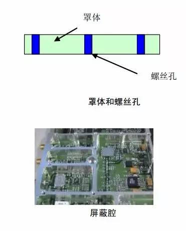 5.2 Process requirements for PCB layout related to metal shielding cavities5.2.1 The design of the shielding cover in contact with the PCB should consider the height of the components on the PCB bottom surface, especially the height of the pins of inserted components.5.2.2 The size of the screw prohibition area should be considered to prevent damage to surface lines or components during assembly. Due to structural size limitations, the size of the PCB for power amplifier boards is relatively small; thus, the screw installation space (prohibition area) is generally required to be at least outside the solder pads. The screw installation space is shown in Table 5.
 5.2.3 The cost of metal shielding covers and assembly costs is high, and irregularly shaped metal shielding covers are difficult to ensure high precision and flatness during manufacturing, which also restricts component layout; metal shielding covers are not conducive to component replacement and fault location.5.2.4 It is crucial to ensure the integrity of the shielding cover; digital signal lines entering the metal shielding cavity should preferably run through inner layers, while RF signal lines can exit from small notches at the bottom of the metal shielding cavity, but as many grounds as possible should be laid around the notches. Grounds on different layers can be connected through multiple vias.5.2.5 To ensure assembly and repair, no components exceeding the height of the shielding cover should be present within a 5mm radius around the shielding cover, and the distance from small chip components to the shielding cover should be more than 2mm, while other components should be more than 3mm away, and their placement should ideally conform to maintenance convenience.5.2.6 No components exceeding the height of the shielding cover should be present inside the metal shielding cavity, and the distance from the tops of components to the shielding cover surface should comply with safety regulations.5.2.7 The height matching between SMA microstrip sockets and PCB should be considered during contact; otherwise, solder reliability may be affected. As shown in Figure 29, the tolerances of the PCB thickness (±10%) and the processing errors of the metal shielding cavity (±0.05mm) should be taken into account. It is recommended that the height gap between the SMA microstrip socket and the PCB should not exceed 0.5mm, and there should be no significant deviation between the socket and the solder pad.
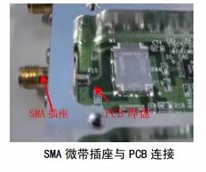 5.2.8 Due to the special circumstances of power amplifier board design, it is permissible for the signal between two boards to pass through the shielding cover and be connected with flying leads, as shown in the figure.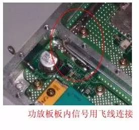
4. RF Traces and Ground
For example, we will conduct RF line simulation on multi-layer circuit boards. To better compare, we will divide the simulated PCB into two sections: before and after the ground is laid on the top layer; the PCB file before the top layer is laid with ground is shown in the diagram below (two line widths): 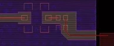 Figure 1a: RF trace with a width of 0.1016 mm (before laying ground on the top layer)
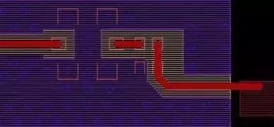 Figure 1b: RF trace with a width of 0.35 mm (before laying ground on the top layer)First, the two boards with different line widths (before laying ground on the top layer) are imported into SIWAVE from ALLEGRO, and a 50Ω port is added to the target line. For the different line widths of 0.1016mm and 0.35mm, our simulation results are shown in Figure 2, where the curves displayed are S21, and the simulation frequency range is 800MHz-1GHz.
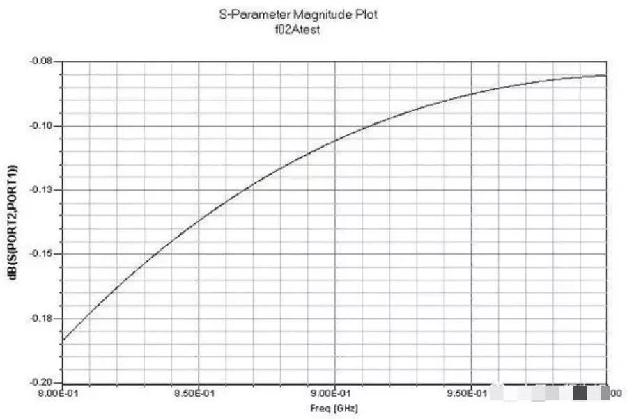 Figure 2a: S21 of the top layer without ground (line width 0.1016mm)
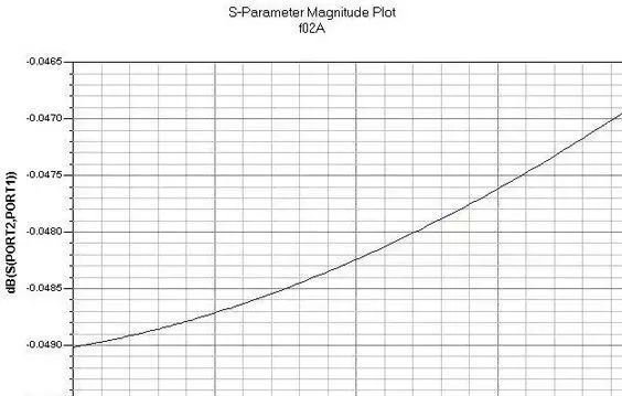 Figure 2b: S21 of the top layer without ground (line width 0.35mm)From the figures, it can be seen that within the range of 800MHz-1GHz, the simulated data shows a magnitude of one to two decimal places, and the loss of 0.35mm is an order of magnitude smaller than that of 0.1016mm. This is because the characteristic impedance of the 0.35mm width trace is close to 50Ω under the stacking conditions of this board. Thus, it indirectly verifies that our impedance calculations (using trace width constraints) have some effect.Next, we conducted the same simulation after laying ground on the top layer (800MHz-1GHz), and the imported PCB file is shown in the diagram below.
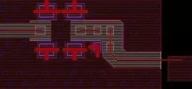 Figure 3a: RF trace with a width of 0.1016 mm (after laying ground on the top layer)
 Figure 3b: RF trace with a width of 0.35 mm (after laying ground on the top layer)Figure 3: PCB after laying ground on the top layerThe simulation results are shown in the diagram below:
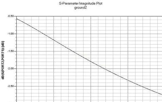 Figure 4a: S21 after laying ground on the top layer (0.1016mm)
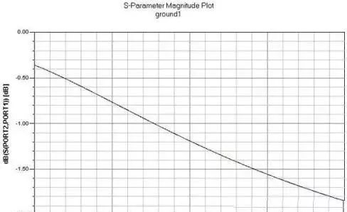 Figure 4b: S21 after laying ground on the top layer (0.35mm)Figure 4: S21 after laying ground on the top layerFrom the figures, it can be seen that the simulated data shows that the line loss of this transmission line is already at the order of 1-2 dB; obviously, the loss of 0.35 mm is significantly smaller than that of 0.1016 mm. Another noticeable phenomenon is that compared to the simulation results without ground, as the frequency increases from 800MHz to 1GHz, the loss tends to increase.From the simulation results, we can draw the following conclusions:1. RF traces should ideally be routed at 50 ohms to minimize line loss;2. Laying ground on the top layer effectively couples some RF signal energy to the ground, causing some loss. Therefore, the ground on the PCB top layer should be carefully considered, ideally kept away from RF lines, with an engineering experience suggesting being more than 1.5 times the trace width.[5] Design Checklist
| Category | Subcategory | Number | Description |
| General | Layout | 1 | ESD protection components should be placed directly on the main signal path. |
| 2 | Module partitioning should be reasonable, with attention paid to the self-resonant frequency of the cavity. | ||
| 3 | The top surface of shielding walls and internal chamfer positions is a prohibition area for layout, routing, and signal vias. | ||
| 4 | Matching components should be placed close to the relevant RF component ports. | ||
| 5 | Thermal design has been considered to ensure heat is not concentrated and can dissipate easily. | ||
| 6 | The main RF signal flow should be laid in a straight line; if space limitations prevent this, an L-shaped layout may be used, but U-shaped layouts should be avoided. | ||
| 7 | The layout of inductors formed by discrete components must ensure that the magnetic field lines of adjacent inductors are perpendicular to each other; if this is not possible for printed line inductors (LTCC process), they should be placed far apart. | ||
| 8 | Combination circuits composed of discrete components should not be disrupted by other components or transmission lines, for example, the three resistors in a resistive attenuator should be placed close together. Filter circuit layouts should be on one side and should not be disrupted by other transmission lines. | ||
| 9 | High, medium, and low-frequency combinations of filters should ensure that high-frequency small-capacity filtering capacitors are closest to the component pins. | ||
| 10 | The number and layout of screws on the PCB should be reasonable. | ||
| 11 | The windowing of the power amplifier PCB has comprehensively considered installation margins and electrical performance. | ||
| 12 | The positions of variable capacitors and coupling capacitors in the power amplifier should be laid out according to the requirements of the schematic designer. | ||
| 13 | The distance between components and the shielding wall should meet the requirements, considering tolerances. | ||
| 14 | Whether the input and output of RF PCBs and other parts meet design requirements. | ||
| 15 | Under normal working or testing environments, there should be no stubs. | ||
| 17 | The PWM modulation output DC filtering circuit of digital chips should be placed on the digital chip side. | ||
| 18 | Cascaded amplifier circuits with a gain exceeding 40dB should be partitioned. For example, the gain of receiving channels is generally very large and requires partitioning. | ||
| 19 | Cascaded attenuation circuits with an attenuation greater than 40dB should be partitioned. | ||
| 20 | Cascaded filtering circuits with out-of-band attenuation and cascaded switching circuits with isolation greater than 40dB should be partitioned. | ||
| 21 | Power supply distribution for RF should generally follow the principle of nearby supply to avoid mutual interference. Additionally, when different chips share the same power supply chip, attention should be paid to whether interference occurs through the power supply. | ||
| 22 | Whether the placement of the power supply is appropriate, ensuring that input and output power supply lines do not cross and the routing distance is minimized. | ||
| 23 | Whether the filtering capacitors at the power supply input are close to the input pins, and arranged in order from largest to smallest, with the smallest capacitance closest to the power supply input pins. | ||
| 24 | Whether the layout meets the special requirements specified in the component datasheets. | ||
| Routing | 1 | Routing RF lines requires impedance control, and they should be routed as directly as possible to minimize losses and unwanted coupling. | |
| 2 | Microstrip lines require continuous ground underneath; similarly, strip lines require continuous ground above and below; the ground plane not only provides necessary return paths but also isolates signals from other signal layers; | ||
| 3 | Long unshielded traces, such as RF front-end connections, should use strip lines, which are favorable for utilizing inherent shielding. | ||
| 4 | Avoid multiple back-and-forth routing on inner and outer layers; | ||
| 5 | When RF signal lines transition between different layers, vias should be kept away from potential interference circuits, routing, and vias (such as digital control lines, clocks, power supplies, etc.); ensure that RF vias and interference paths have ground laid and grounded vias for isolation. | ||
| 6 | The distance between clock lines, data lines, and control lines must meet the 3W principle. If space allows, try to increase the distance between lines. | ||
| 7 | Routing should be as short as possible, with no loops, and no sharp angles or right angles. | ||
| 8 | No vias or routing should be below the crystal oscillator surface. No routing should occur under frequency synthesizers, PLL filter components, VCOs, filters, and inductors. | ||
| 9 | Analog signals and digital signals, power lines and control signal lines, weak signals and any other signals need to be layered (preferably with ground isolation) or routed far apart. If there are no layered lines, the distance between lines must meet isolation requirements, at least greater than 3W. | ||
| 10 | RF sensitive signals should not be placed near strong radiation signals. | ||
| 11 | Differential signal lines should be routed symmetrically, with a length difference not exceeding 100mil, and the spacing between differential lines should meet the 3W rule. | ||
| 12 | Devices with input and output impedances not equal to 50 ohms should meet impedance matching requirements for input and output lines. | ||
| 13 | In the schematic, lines with special impedance requirements should meet the design requirements of the schematic. | ||
| 14 | During routing of power lines for different units, power lines should be isolated from each other to prevent mutual interference through the power supply. | ||
| 15 | Different power supply layers should not overlap in space; if overlapping is necessary, ground layer isolation should be provided. | ||
| 16 | The width of power supply routing should meet the current carrying requirements (generally referenced as 1A/mm width). | ||
| 17 | If other RF signal lines exist around RF signal routing, grounding copper foil should be added between them, with grounded vias. | ||
| 18 | The number of vias for power supply printed lines transitioning between layers should meet the current carrying requirements (1A/Ф0.3mm vias). | ||
| 19 | If other unrelated non-RF signals (such as power lines) exist around RF signal routing, grounding copper foil should be added between them, with grounded vias. | ||
| 20 | Power supply routing for small signal amplifiers needs to be isolated with ground copper foil and grounding vias to prevent other EMI interference from entering and deteriorating the signal quality of this stage. | ||
| 21 | Grounding lines should be short and straight to reduce distributed inductance and minimize interference caused by common ground impedance. | ||
| 22 | Grounding devices and power filtering capacitors on the main RF signal path need to be grounded closely to reduce the grounding inductance of the devices. | ||
| 23 | Some components have metal shells grounded at the bottom; grounding holes should be added within the projection area of the components, and no signal lines or vias should be routed on the surface layer; | ||
| 24 | When grounding lines need to travel a certain distance, the width of the routing should be increased, and the routing length should be shortened, prohibiting approaching or exceeding 1/4 of the guiding wavelength to prevent antenna effects from causing signal radiation; | ||
| 25 | Except for special purposes, isolated copper foil should not exist, and grounding vias must be added to the copper foil. | ||
| 26 | For certain sensitive circuits or circuits with strong radiation sources, they should be placed inside shielding cavities, and the shielding cavity should be pressed against the PCB surface during assembly. During design, “via shielding walls” should be added, which are grounding vias at the locations on the PCB that are in close contact with the walls of the shielding cavity. There should be more than two rows of vias, staggered, with the spacing between the vias in the same row around 100mils. | ||
| 27 | Some RF devices have small packages, with SMD pad widths possibly as small as 12mils, while RF signal line widths may exceed 50mils; gradual lines should be used, and abrupt width changes are prohibited, with the transition section not being too long. | ||
| 28 | When there are large pads on a 50 ohm microstrip line, the large pads act as distributed capacitance, disrupting the continuity of the characteristic impedance of the microstrip line. The ground plane below the pads should be excavated to reduce the distributed capacitance of the pads, and simulations should be conducted to ensure the impedance is 50 ohms. | ||
| 29 | Vias are one of the important factors causing impedance discontinuity on RF channels; if the signal frequency exceeds 1GHz, the impact of vias must be considered. Specific situations require optimization simulations using HFSS and Optimetrics. | ||
| RF Module | Frequency Source Module | 1 | Data, clock, and enable lines should not be routed on the surface layer beneath digital frequency synthesizer chips, crystals, oscillators, transformers, optocouplers, power modules, and other devices. |
| 2 | Power supply lines for frequency synthesizers should be isolated from other interference signals to avoid affecting the phase noise and spurious of the frequency synthesizer. | ||
| 3 | The layout of loop filters should be on the same layer and compact, close to relevant filtering pins, with no routing on the bottom surface of the filter. | ||
| 4 | The power and control voltage for VCO should be isolated from other interference signals. | ||
| 5 | No routing should occur beneath the VCO. | ||
| 6 | The distances between data, clock, and enable signals for frequency synthesizers should meet at least a 3W spacing requirement. If layered routing is used, they should not overlap in parallel. | ||
| Reference Source Module | 1 | The reference input signal for the reference source is sent from the intermediate frequency, and the routing should be kept short to avoid affecting other circuits. | |
| 2 | The distances between data, clock, and enable signals should meet at least a 3W spacing requirement. If layered routing is used, they should not overlap in parallel. | ||
| 4 | The power and control voltage for VCO should be isolated from other interference signals. | ||
| 5 | The output circuit of the reference source should be isolated from other signals. | ||
| LNA Module | 1 | The input signal line for the LNA should be as short as possible to reduce line loss and enhance the sensitivity of the receiving channel. | |
| 2 | The matching circuit for the LNA should be placed close to the corresponding pins. | ||
| 3 | The ESD protection circuit for the RF front end should be placed on the main trunk line of the RF signal to prevent reducing the protection level. | ||
| Small Signal Amplifier Module | 1 | The power supply routing for small signal amplifiers needs to be isolated with ground copper foil and grounding vias to prevent other EMI interference from entering and deteriorating the signal quality of this stage. | |
| 2 | The solder pads for the bias inductors of single-chip amplifiers should also be placed on the RF signal line; if space is tight, they can be connected to the RF signal line through a 12mil high-resistance line. | ||
| 3 | When two stages of amplifiers are powered by the same power supply, the power should be supplied from the last stage to the front stage to avoid the last stage amplifier circuit affecting the front stage. | ||
| 4 | The grounding loop for the power supply of small signal amplifiers should be small, and the capacitor grounding should be short and straight to minimize interference caused by common ground impedance. | ||
| Filter Module | 1 | The matching components of the filter should be placed close to the corresponding pins. | |
| 2 | When the input and output pins of the filter are large pads, to ensure the continuity of impedance, the layers beneath the pads need to be excavated. Specific impedance values need to be calculated through simulation software. | ||
| 3 | When the bottom of the filter is connected to the grounding pin of a metal shell, the projection area of the component is a prohibition area for routing microstrip lines and vias. | ||
| Integrated Mixer | 1 | The peripheral components of the mixer should be laid out according to the requirements of the datasheet. | |
| 2 | For integrated double-balanced mixers, choke inductors and isolation inductors must be placed far apart and vertically positioned. | ||
| 3 | For integrated double-balanced mixers, the grounding of isolation inductors must be sufficient, with additional grounding vias placed nearby. | ||
| 4 | For integrated double-balanced mixers, the two choke inductors should be symmetrically and parallelly placed. | ||
| Integrated Modulator | 1 | I/Q consists of two pairs of differential lines, and the spacing between these pairs must meet the 3W rule, with grounding vias added for isolation. | |
| 2 | I/Q consists of two pairs of differential lines, and these pairs should be routed in parallel without crossing each other. | ||
| 3 | The length difference of the two pairs of differential lines should not exceed 100mil. | ||
| 4 | The number of vias for routing differential lines should not exceed 4. | ||
| Power Supply Circuit | RF Power Supply | 1 | The power supply line is an important pathway for EMI to enter and exit the circuit. Through the power supply line, external interference can enter the internal circuit, affecting RF circuit indicators. To reduce electromagnetic radiation and coupling, it is required that the loop area on the primary side, secondary side, and load side of the DC-DC module be minimized. Regardless of how complex the power supply circuit is, its large current loop should be kept as small as possible. |
| 2 | Long-distance power supply lines on the same board should not be close to or cross near the output and input terminals of cascaded amplifiers (gain greater than 45dB). This is to avoid the power supply line becoming a transmission path for RF signals, which may cause self-excitation or reduce sector isolation. High-frequency filtering capacitors should be added at both ends of long-distance power supply lines, and even in the middle. | ||
| 3 | The power supply entrance of RF PCBs should combine three filtering capacitors in parallel, utilizing the advantages of each of these capacitors to filter out low, medium, and high frequencies on the power supply line. For example: 10uF, 0.1uF, 100pF, and arranged in order from largest to smallest, closest to the input pin of the power supply. | ||
| 4 | When using the same group of power supplies to power small signal cascaded amplifiers, the supply should start from the last stage and proceed to the front stage, to minimize the impact of EMI generated by the last stage circuit on the preceding stage. Each stage’s power supply filtering should have at least two capacitors: 0.1uF and 100pF. When the signal frequency exceeds 1GHz, a 10pF filtering capacitor should be added. | ||
| 5 | Different power supply layers should avoid overlapping in space. This is mainly to reduce interference between different power supplies, especially between power supplies with significant voltage differences; the overlapping issue of power planes should be avoided as much as possible, and if unavoidable, consider using an intermediate ground layer. | ||
| 6 | The number of vias for power supply printed lines transitioning between layers should meet the current carrying requirements (1A/Ф0.3mm vias). | ||
| 7 | The copper foil size of the POWER section of the PCB should meet the maximum current flowing through it, considering a margin (generally referenced as 1A/mm width). | ||
| 8 | The input and output of the power supply lines should not cross. | ||
| Other | Safety Regulations | 1 | The number of vias for power supply printed lines transitioning between layers should meet the current carrying requirements (1A/Ф0.3mm vias). |
| 2 | The copper foil size of the POWER section of the PCB should meet the maximum current flowing through it, considering a margin (generally referenced as 2A/mm width). | ||
| 3 | Protection and thermal treatment measures for high-temperature components on the board should be reasonable (similar to high-temperature component handling for heating devices). | ||
| 4 | Large-area accessible conductive components should be connected to ground (such as DC/DC shells, shielding boxes). | ||
| 5 | The fixing holes and electrical clearance of large components after installation should meet safety regulations (such as DC/DC shells, shielding boxes). | ||
| 6 | After fixing the shielding box, the electrical clearance with other connectors that carry hazardous energy or with high-voltage electrodes should meet safety regulations; the distances of fixing screws and washers on the printed board should comply with requirements. | ||
| 7 | -48V input printed lines should not be located in overlapping positions, and the interlayer distance should not be less than 0.1mm. | ||
| 8 | The connectors in the power supply section of the PCB should have measures to prevent reverse insertion. | ||
| 9 | The printed lines of DC/DC input/output should not be on the same surface as the DC/DC module (except for surface-mounted DC/DC; non-stepped DC/DC shells may not provide sufficient electrical clearance with printed lines and may rely on solder mask for insulation). | ||
| 10 | The output of the power amplifier should have a protection circuit (such as a circulator) to ensure that it does not exceed power and cause overheating or burning events. | ||
| 11 | The wiring between lightning protection connectors and gas discharge tubes and protection diodes should be as thick as possible, and the distance to ground should be greater than 80mil. |
1. Layout Considerations(1) Structural design requirements: Before PCB layout, it is necessary to clarify the product’s structure. The structure needs to be reflected on the PCB. For example, the thickness of the outer wall of the casing, the thickness of the internal cavity, the radius of the chamfer, and the size of screws on the cavity, etc. (In other words, structural design is based on the outline (structural part) drawn on the completed PCB). Generally, the outer wall thickness is 4mm; the inner cavity width is 3mm; for glue dispensing processes, it is 2mm; and the chamfer radius is 2.5mm. Taking the lower left corner of the PCB as the origin, the cavities should be on a grid of integer multiples of 0.5, with a minimum requirement of integer multiples of 0.1. This facilitates processing by structural manufacturers and allows for more precise error control. Of course, this needs to be designed according to customer requirements.The diagram below shows the structural outline after PCB design is completed:(2) Layout requirements: The RF link should be prioritized for layout, followed by other circuits. A. Layout considerations for RF links: The layout should be strictly based on the order of the schematic (from input to output, including the sequence and spacing between each component). Some components should not be too far apart, such as π networks. The layout should be either linear or L-shaped. In actual RF link layouts, due to product space limitations, it is impossible to achieve this completely, which forces us to layout in a U-shape. While U-shaped layouts are not prohibited, a cavity should be added in the middle to isolate the left and right sides, ensuring proper shielding.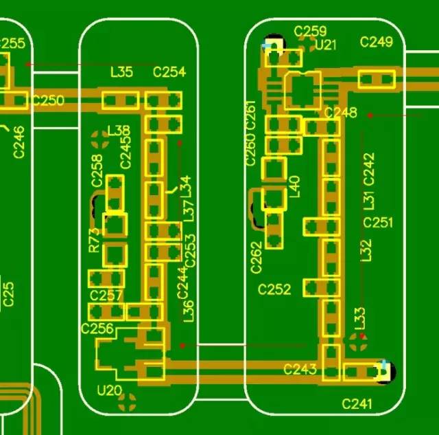 Another method requires adding cavities laterally, i.e., using cavities to isolate the left and right sides of a linear layout. This is mainly because certain sensitive parts need to be isolated or may interfere with other circuits; additionally, if the gain from the input to the output of a linear circuit is too large, cavities are required to separate them (if the gain is too high, the cavity may be too large and could cause self-excitation).
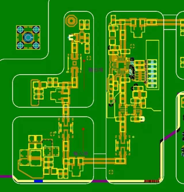 B. Layout of peripheral circuits around chips: The layout of peripheral circuits for RF devices should strictly follow the requirements in the datasheet, with adjustments made for space limitations; the layout of peripheral circuits for digital chips will not be elaborated on here.2. Routing ConsiderationsRouting should be based on 50-ohm impedance line widths, ideally starting from the center of the pad in straight lines, preferably on the surface layer. At points where bends are needed, 45-degree angles or curved routing should be made, preferably around capacitors or resistors. If there are matching requirements for component routing, the lengths of the traces should strictly follow the reference values in the datasheet. For example, the routing length between an amplifier and a capacitor (or the routing length between inductors) should be considered, etc.During PCB design, to make the high-frequency circuit board design more reasonable and improve anti-interference performance, the following aspects should be considered (general practices):(1) Reasonable selection of the number of layers: In PCB design for high-frequency circuit boards, using inner plane layers as power and ground layers can provide shielding, effectively reducing parasitic inductance, shortening signal line lengths, and lowering cross-interference between signals.(2) Routing methods: Routing must involve 45° angles or curved bends to reduce the emission of high-frequency signals and mutual coupling between them.(3) Trace lengths: Shorter trace lengths are better, and the distance between two parallel lines should also be minimized.(4) Number of vias: The fewer vias, the better.(5) Inter-layer routing direction: The inter-layer routing direction should be vertical, with the top layer being horizontal and the bottom layer being vertical to minimize interference between signals.(6) Copper pouring: Increasing grounding copper pouring can reduce interference between signals.(7) Grounding: Important signal lines should be grounded to significantly improve the anti-interference capability of those signals; of course, interference sources should also be grounded to prevent them from interfering with other signals.(8) Signal lines: Signal routing should not form loops and should follow a daisy chain layout.3. Grounding Treatment(1) RF link grounding: The RF part should use a multi-point grounding method for grounding treatment. The copper spacing for RF link copper pouring is generally 30mil to 40mil. Both sides should have grounding vias, and the spacing should be kept as consistent as possible. Grounding pads for capacitors and resistors on the RF path should have grounding vias placed as close as possible.
 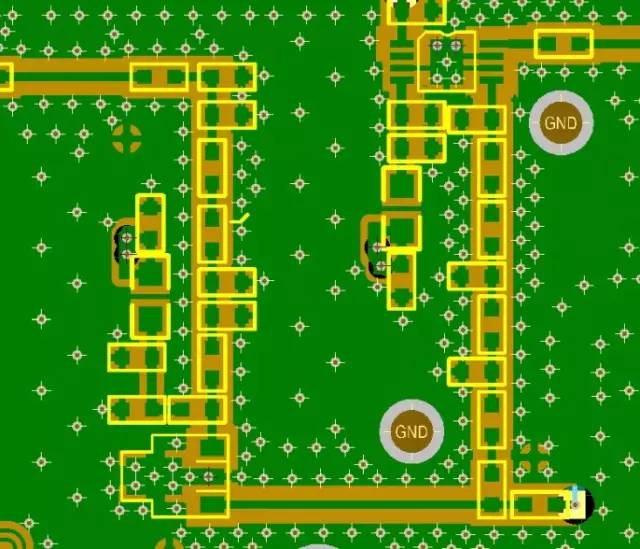 (2) Grounding vias for cavities: To ensure better contact between the cavity and the PCB, generally two rows of grounding vias should be placed in an alternating manner, as shown in Figure 06. Windows need to be opened on the PCB cavities, as shown in Figure 07. The grounding copper foil on the PCB bottom layer should have windows opened at the contact points with the bottom plate for better contact, as shown in Figure 08 (the upper half of the PCB is in contact with the base):
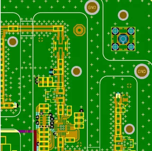 PCB cavity grounding via diagramPCB cavity window opening diagram
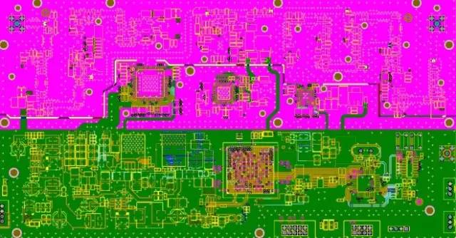 PCB bottom layer window opening diagram(3) Screw placement (requires structural knowledge): To ensure tighter contact between the PCB and the base and cavity (better shielding), screw holes should be placed on the PCB. The screw placement method between the PCB and the cavity: a screw should be placed at each intersection of the cavity. In actual design, this is relatively difficult to achieve, and adjustments can be made based on the functional requirements of the module circuit. However, the four corners of the cavity must have screws.
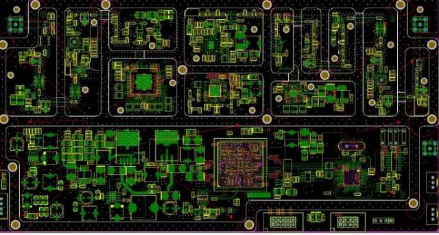 Cavity screw diagramThe screw placement method between the PCB and the base: each small cavity within the cavity should have screws, depending on the size of the cavity (the larger the cavity, the more screws should be placed). The general principle is to place screws diagonally across the cavity. Screws must also be placed next to SMA heads or other connectors to prevent PCB deformation during the insertion and removal process.
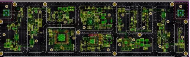 Cavity internal screw diagramDisclaimer:This article is reproduced from the Electronic Kaleidoscope; if there are issues related to the content, copyright, or other matters, please contact the staff via WeChat (prrox66), and we will coordinate with you for deletion processing!Submissions/Recruitment/Advertising/Course cooperation/Resource exchange Please add WeChat: 13237418207