Today, we continue to introduce the basic principles of exposure and development in outer layer pattern transfer.
4.3 Exposure
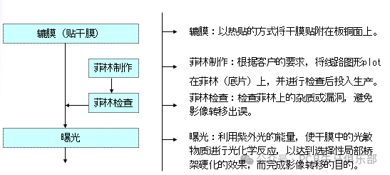
Definition: Using photosensitive materials, the designed circuit patterns are achieved through the processes of exposure/development/etching to obtain the desired copper circuit patterns.
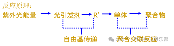
Reaction Principle:
Exposed Area:
The area of the film that is transparent under ultraviolet light causes the photoinitiator to absorb light energy and decompose into free radicals. These free radicals then initiate the polymerization of light-sensitive monomers, resulting in a large molecular structure that is insoluble in dilute solutions.
Unexposed Area: The area of the film that is opaque will maintain its adhesion after the film is applied and will be washed away by the developer.
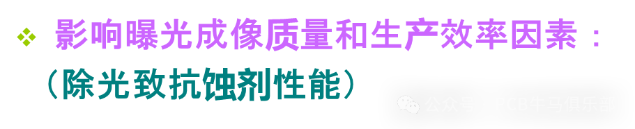
1) Exposure Machine Light Source 2) Exposure Energy
3) Dry Film Characteristics
4) Quality of the Film
1) Selection of Exposure Light Source
The characteristics of the light source directly affect the quality and efficiency of exposure. The spectrum emitted by the light source should match the absorption spectrum of the photosensitive material to achieve better exposure results. Currently, the absorption wavelength of dry film is 325-365nm, and shorter wavelengths result in clearer and sharper edges of the imaged patterns.
The relationship between light energy and wavelength is as follows:
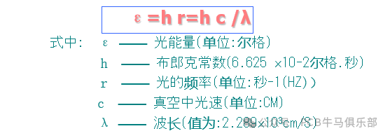
From the equation, it can be seen that the shorter the wavelength of light, the greater its energy. Since wavelengths below 300nm are easily absorbed by glass and polyester film bases, the light sources used in exposure machines generally have wavelengths between 320-400nm. High-pressure mercury lamps and halogen lamps have significant relative radiation intensity in the 310-440nm wavelength range, making them ideal light sources for dry film exposure.
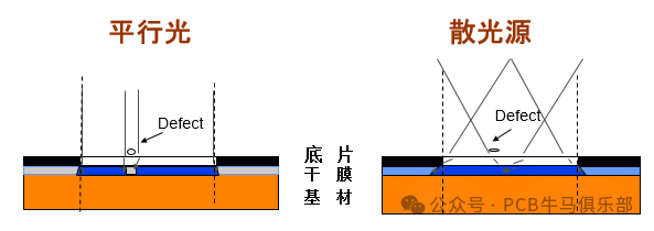
Types of exposure light sources include scattered light and parallel light:
In fact, a completely ideal parallel light exposure machine does not exist, but we often use the incident angle θc (Declination Angle) and the scattering angle θα/2 (Collimation Angle) of the exposure machine’s light source to determine its performance.
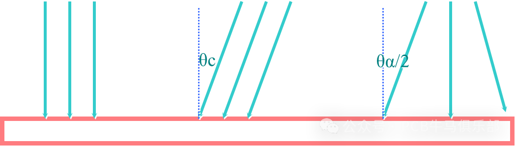
The general definition of a parallel light exposure machine: θc, θα/2 ≤ 30
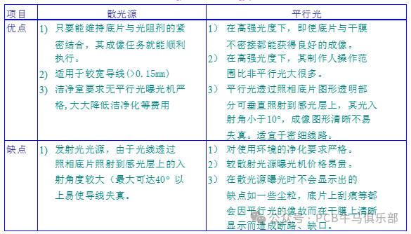
Comparison of the advantages and disadvantages of scattered light and parallel light:
2) Control of Exposure Energy:
During the exposure process, the polymerization reaction of the dry film is not initiated instantaneously, but generally goes through three stages:
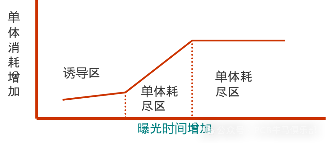
Therefore, correctly controlling the exposure time is one of the main factors in obtaining excellent dry film resist images.
Determination of Exposure Energy:
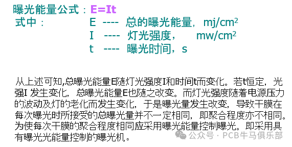
Determination of Exposure Time:
Using a Ristor 17 grid or SST21 grid exposure gauge for exposure imaging checks to determine exposure time. When using a light density gauge, lower light density (i.e., more transparent) levels allow the dry film to absorb more ultraviolet energy and polymerize more completely, while higher light density (i.e., less transparent) levels result in less ultraviolet energy absorption, leading to incomplete polymerization or no polymerization at all. By selecting different exposure times, different imaging levels can be obtained, which will be washed away or partially retained during development.
4.3 Dry Film Characteristics (Photoresist Dry Film)
1) Structure of Dry Film
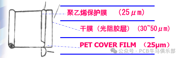
Among them: The polyethylene protective film covers the photosensitive resin layer to prevent dust and other contaminants from adhering to the dry film, thus preventing the dry film resin layer from adhering to the underlying PET;
The role of the transparent polyester cover (PET):
1. Prevents the dry film resist layer from being scratched before exposure;
2. During exposure, it prevents oxygen from entering the photoresist layer, which would destroy free radicals and reduce sensitivity.
2) Main Components and Functions
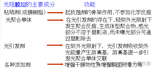
3) Composition of the Main Resin in the Photosensitive Layer
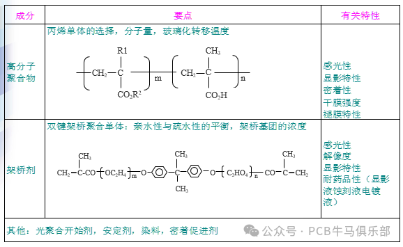
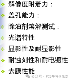
3) Main Quality Requirements for Dry Film Usage:
4.4 Pattern Transfer Tools
When using dry film as the image transfer medium for circuit boards, silver halide film or diazo film is required as the exposure tool, acting as the “negative” during exposure, with diazo film being formed from silver halide film through exposure. With the development of PCB technology, the level of automation has increased, leading to a wider use of silver halide film. However, diazo film is used less frequently due to deformation and other issues during the copying process.
Most leading companies now use LDI (Laser Direct Imaging) technology, also known as “electronic film,” resulting in a decreasing use of physical films (negatives) such as diazo film and silver halide film, which are gradually becoming obsolete.
The main factors affecting the quality of film negatives are light density and dimensional stability.
Light Density Requirements:
Maximum light density D max greater than 4.5;
Minimum light density D min less than 0.2
* Maximum light density refers to the opacity of the negative under ultraviolet light, where the opaque area must exceed a light density of D max greater than 4.5 to achieve good opacity.
* Minimum light density refers to the upper limit of transparency outside the opaque film under ultraviolet light, where the transparent area must have a light density of D min less than 0.2 to achieve good transparency.
Dimensional Stability Impact:
The dimensional stability of the negative directly affects the dimensional accuracy and image registration of the printed circuit board, influenced by changes in temperature, humidity, and storage time.
The table below shows the dimensional changes of D1A20 (determined by expansion coefficient data).
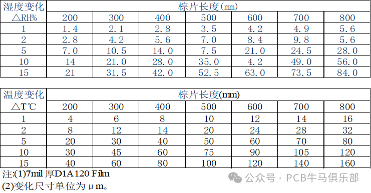
From the table, it can be seen that between 0-50℃ and 10-90RH, using 7mil D1A20 as an example, the average change per △%RH is 0.7×10⁻⁵, while each △T ℃ changes approximately 2 ×10⁻⁵. If this change does not exceed the limit, when the temperature and humidity return to their original state, the dimensions of the D1A20 film will return to their original size.
To ensure that the D1A20 negative achieves equilibrium with the temperature and humidity of the working environment, it should be allowed to stand in the manufacturing area for at least 8 hours before exposure.
Due to the influence of film dimensional stability and other factors, direct laser imaging technology (LDI) has been developed that does not require film.
Exposure Room Environmental Control
To manufacture high-quality PCB boards, it is essential to create an excellent working environment, and the pattern transfer room must be established as a clean room.
A clean room is classified based on the number of particles greater than 0.5 microns per cubic foot of air (PPOF), divided into three levels:
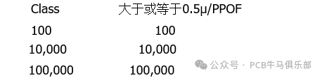
Note: The classification standard is based on the U.S. Federal Standard Fed STD 209B.
Environmental Control Requirements for the Exposure Room:
1. Temperature and Humidity Requirements:
Temperature: 21.5 ±2℃,
Humidity: 53 ±3RH%
2. Establishment of a “Clean Room”:
Purification level reaches 10K-100K level
3. Lighting Source Requirements:
Since the wet film is a photosensitive material, yellow light should be used in the working area.
4.4 Development Principle:
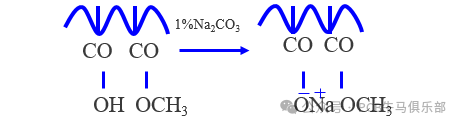
The principle of removing the unpolymerized dry film layer with Na2CO3 solution is that it forms sodium salt and dissolves, while the exposed part does not form sodium salt and is preserved.
To be continued!!! This is Part 2
Special Note: The above discussion is for reference only and serves as a starting point for further exploration! Each factory’s chemicals/processes/equipment/product structures, etc., have various differences, and one must not rigidly apply these principles. All effective improvement measures come from experimental data! As a professional quality of engineering technicians, it is essential to “speak with data.”
This public account will continue to update information related to PCB manufacturing and cutting-edge technology.
Thank you for being not only good-looking and handsome but also able to move your golden fingers to make money. Please follow, collect, like, share, and comment!!! Follow us so you won’t get lost!!!
Original content is not easy to produce. If you want to reprint, please message the author for permission and indicate the source before reprinting. Thank you for your cooperation!