Panelization refers to the process of combining multiple small PCB boards into a single larger panel by the manufacturer.
1. Why Panelize? What Are the Benefits of Panelization?
1. To meet production needs. Some PCB boards are too small to meet the requirements for fixtures, so they need to be panelized for production.
2. To improve the soldering efficiency of SMT assembly. Multiple PCBs can be soldered in one pass through the SMT.
3. To enhance cost efficiency. Some PCB boards are irregularly shaped, and panelization can more efficiently utilize the area of the PCB, reducing waste and improving cost efficiency.
2. What Are the Different Panelization Designs?
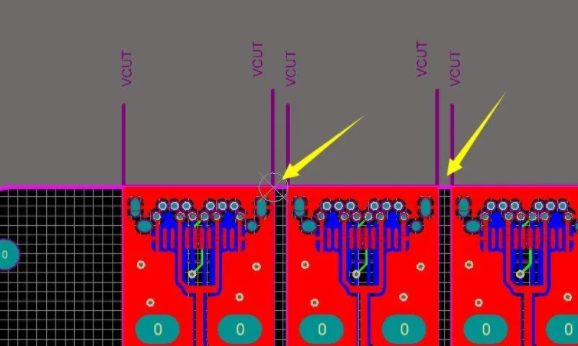
V-CUT involves creating a groove at the connection point of two boards; as long as the two boards are aligned with a small gap (usually 0.4mm), this area will be relatively thin and prone to breaking, so care must be taken to merge the edges of both boards during panelization.
V-CUT is generally linear, avoiding complex curves or arcs, and should ideally be aligned in a straight line during panelization.
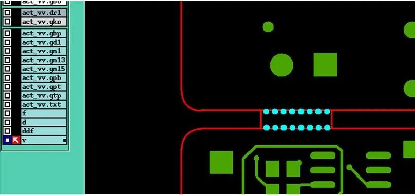
For irregular PCB boards, such as circular ones, V-CUT cannot be used. In this case, stamp holes are utilized for panel connections, making them more common in irregular boards.
Two boards are connected through a small piece of material that has several small holes at the connection points, making it easier to break. Once broken, the edges of the boards resemble the edges of a stamp, hence this panelization method is called stamp hole.
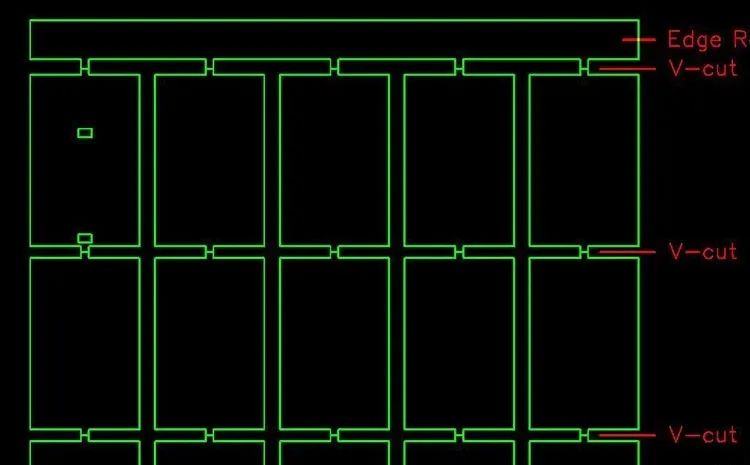
3. Hollow Connecting Strip
The hollow connecting strip is often used in boards with semi-hole technology, utilizing very narrow material for connection. It is somewhat similar to the stamp hole, but the connecting part of the strip is narrower, and there are no through holes on either side.
A disadvantage of the hollow connecting strip method is that there will be a noticeable bump after breaking the board. The stamp hole also has a bump, but it is less noticeable due to being separated by the through holes.
Some may wonder why not just use the stamp hole; why use the hollow connecting strip? This is because when creating modules with semi-hole technology on all sides, neither the stamp hole nor V-CUT can be used, and only the hollow connecting strip can connect at the four corners of the module.
3. What Are the Principles of Panelization?
To facilitate production, the panelized board should ideally maintain a square shape. In short, the aspect ratio should not be too disparate.
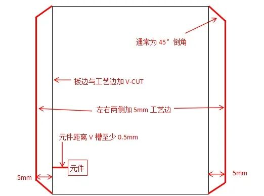
1. For PCBs where the outermost component is less than 3mm from the board edge, a process edge must be added, typically using the longer edge as the process edge;
2. A space greater than 0.5mm should be reserved between components and V-CUT to ensure normal operation of the cutting tool.
Copyright statement: The copyright of this article belongs to the original author and does not represent the views of the association. The articles pushed by the “Jiangxi Province Electronic Circuit Industry Association” are for sharing purposes only and do not represent the position of this account. If there are copyright issues, please contact us for deletion.