Remember to star the public account ⭐️ to receive notifications promptly.

Source: Content compiled from semiengineering.
Advanced packaging is becoming a key differentiator in the high-end mobile market, enabling higher performance, greater flexibility, and faster time-to-market compared to system-on-chip (SoC) solutions.
Single-chip SoCs are likely to remain the preferred technology for mid-range and low-end mobile devices due to their compact size, mature experience, and lower costs. However, multi-chip components offer greater flexibility, which is crucial for AI inference and keeping pace with the rapid changes in AI models and communication standards. Ultimately, OEMs and chip manufacturers must determine how to adapt to changes within the design cycle and which market segments to target.
Hezi Saar, Executive Director of Mobile, Automotive, and Consumer IP Product Management at Synopsys and Chair of the MIPI Alliance, stated: “SoC vendors not tied to mobile manufacturers must pursue IoT SoCs with AI capabilities at the low end, which will certainly be single-chip. If they need to enter the mid-range mobile market, their capabilities will be higher than those for IoT. It could also be a single-chip [SoC] and may be expanded through multi-chip technology. As you move towards the high end, it is clear that you cannot rely solely on single-chip technology. You need to have the capability to manufacture multi-chip solutions to adapt to upcoming changes and rapid time-to-market, as that is where they truly make their profits.”
In other words, the target market determines the architecture. “We see multi-chip 3D technology as a trend, and the mobile sector is adopting this technology, but its development is much slower than that of NVIDIA or AMD’s HPC chips, which have invested heavily in 3D and 2.5D technologies, with systems containing up to 12 chips,” said Marc Swinnen, Director of Product Marketing at Ansys. “Low-end mobile devices cannot achieve this due to cost issues. They must focus on integrating as many functions as possible into a small-sized single chip while achieving low power consumption and high speed.”
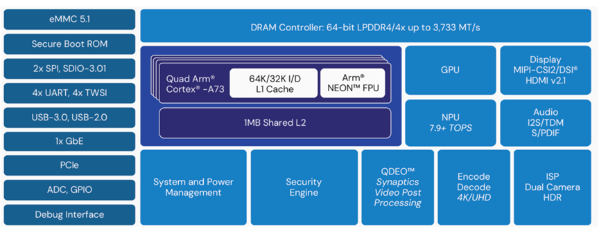
According to Infineon, a single-chip SoC contains all the components necessary to run a system on a single silicon die, which may include an embedded microcontroller with one or more processor cores; memory systems such as RAM or ROM; external interfaces like cable ports (USB, HDMI); wireless communication (WiFi, Bluetooth); graphics processing units (GPUs); and other components such as analog/digital converters, voltage regulators, and internal interface buses.
Despite their compact size (often a reason for their efficiency), single-chip SoCs are extremely efficient, with single-processor performance often surpassing that of more complex systems. The short signal transmission distance requires less power to drive these signals, and only a simple heatsink is needed for cooling. Many IoT SoC vendors adopt a single-chip strategy as it saves customers on packaging and integration costs.
Ananda Roy, Senior Product Manager for Low-Power Edge AI at Synaptics, stated: “While it is challenging, it is always better to put all functions on a single chip. This gives us a competitive advantage because some of our IoT competitors put two chips in one package, either stacked or placed side by side, and call it a single-chip solution. But in reality, they are just two different chips in one package. We consciously try to move towards single-chip solutions because, from the customer’s perspective, it is easier to integrate and fits better into their hardware system design. We essentially build multiple technologies on a single chip.”
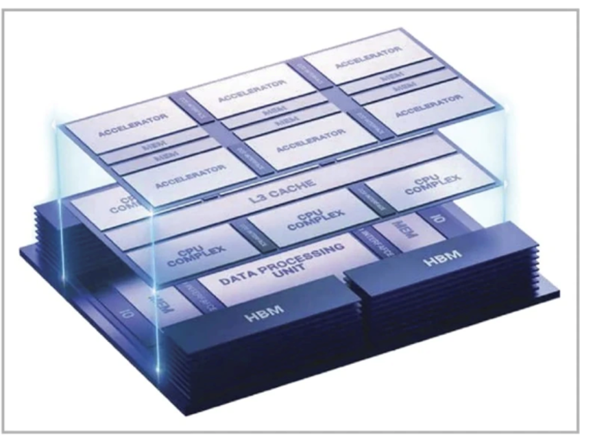
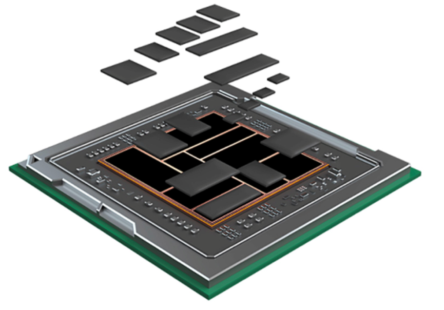
In the high-end mobile market, the situation is quite different. This market uses multiple chipsets to enhance performance and employs more interconnections to reduce resistance and capacitance. Mick Posner, Senior Product Director at Cadence’s Computational Solutions Division, stated: “In this case, the computing engine is ‘mirrored’ and connected through high-performance chip-to-chip interfaces and advanced packaging technologies to expand computing processing capabilities. Technically, this can extend to vertically stacking chips in a 3D-IC stack, achieving higher interconnect bandwidth.”
Multi-chip components also allow for greater diversity in computing units, including combinations of CPUs and GPUs, as well as highly specialized accelerators. Posner stated: “3D stacking is not limited to the same processing units. AI or memory accelerator units can be part of the stack, creating efficient application engines for specific domains. With advanced 3.5D packaging, it is also possible to use more traditional chip-to-chip interconnects (such as UCIe) to connect another chip horizontally. Other chips do not need to be on the same technology node as the processing node. The integration of various nodes can balance performance and cost while selecting the most suitable nodes for application functionality or supply chain flexibility.”
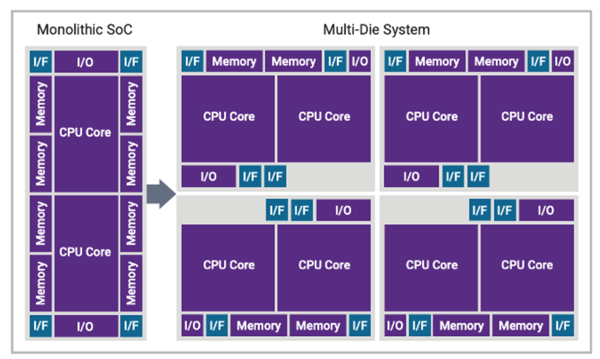
In the early decades of the millennium, the mobile market drove the development of many cutting-edge technologies. However, as the advantages of planar scaling in the finFET era diminish, SRAM cannot be scaled, and the demand for massive computing power in the cloud continues to grow, system companies have shifted from single-chip SoCs to 2.5D systems, connecting multiple chips through an intermediary layer. While the mobile market still leads in process scaling, the high-end mobile market has surpassed this level, expanding into multi-chip assembly—though it remains unclear whether mobile devices will adopt 3D-IC, as they require some form of advanced cooling system, which is not practical in today’s mobile devices.
Saar from Synopsys stated: “2.5D is very fast, highly efficient, and has very short distances, so power consumption is very high. These chips can be manufactured using different processes. This chip can be 2nm (the base chip), while the AI accelerator can be another chip. They are very flexible.”
High-end mobile devices are moving towards 2nm gate-all-around (GAA) manufacturing processes to achieve high performance, but this process is costly and time-consuming. Saar stated: “The GAA process takes X months to return from the wafer fab. You need to compress all this time, which is the biggest challenge. What you are tape-outting was worth mass production in the past. This time, you know you need at least one more tape-out, and while you are doing that, the specifications may evolve again. I originally thought I needed 7 billion parameters. Now I need 14 billion parameters because the use cases for mobile phones have changed. I don’t know what the future will look like, but they need to consider this when introducing these features. That is why multi-die seems to be the right answer to address flexibility, uncertainty, and the continuous evolution of specifications, as well as the market risk mitigation measures you must take.”
Saar pointed out that each mobile manufacturer can decide how to deploy AI based on the number of markets they want to target. “You can integrate an AI accelerator, or you can put it on a separate chip, or it can be a dedicated chip, or even several dedicated AI accelerators. It depends on the performance you want. Suppose I want a base chip for feature phones. I add an AI accelerator chip, which corresponds to a 3D connection between the two. Now, I add another chip on the side of the chip, say, for I/O expansion, because I want to enter the multimedia market. Now I need more display capabilities. I need EDP (Embedded DisplayPort). SoC manufacturers can sell the base chip (independent, single-chip) to the feature phone market. They can add accelerators. Now it becomes a smartphone configuration, and they can add another chip on the side of the chip. Then it becomes a consumer device, super robot, or PC, and they can leverage all these configurations to enter different markets.”
By placing the AI accelerator on a second chip, vendors can achieve better performance as it is optimized while still using the same base. “Now, it no longer needs to spend hundreds of millions of dollars repeatedly spinning silicon, but it has become more stable,” Saar said.
Another reason for adopting multi-chip is the consideration of analog and digital signals. For example, Synaptics’ touch controller for foldable mobile OLED displays can distinguish between holding the device, pocket dialing, water drops, or sweat. “Our chip contains an analog chip and a digital chip, with the analog chip directly connected to the sensor, and the digital chip processing all this information,” said Sam Toba, Product Marketing Director at Synaptics. “Inside the digital chip, we have an MCU core; previously, we had an internally customized MCU core, which had many advantages. But once it comes to these foldable devices, the amount of information to be processed becomes very, very large, so we decided to use RISC-V. Si-Five’s E7 is a very powerful MCU core, well-suited for high-level processing, and our vector co-processor is located outside of it.”
Then, AI/ML algorithms can determine the environment and detect real finger touches. “Our chip connects to the touch sensor, detects all signals, inputs the analog signals into the analog chip, and then processes them on the digital chip,” Toba said. “The digital chip contains E7, Hydra, all algorithms, and memory. Once the chip determines that the touch is meaningful and intentional, it reports to the host SoC.”
Complexities of Memory and Communication
Like AI, memory is also evolving and will vary across different markets. Saar stated that if an SoC vendor targets all markets, they have several ways to achieve this. “They can make single-chip solutions. But how do they adapt to multiple spins of silicon? They now have LPDDR 6, which is already defined, but it will continue to evolve. UFS 5.0 is now defined, but it will continue to evolve. So, will they spin another 2nm silicon? Or will they limit it in other ways?”
There are also various networks to consider. Mobile chips need to be flexible enough to support new 5G/6G protocols while continuing to support older technologies. “Supporting additional bandwidth in a single system increases the complexity of data processing and also means a lot of power consumption, so you must implement it very efficiently,” said Andy Heinig, Head of Efficient Electronics at Fraunhofer IIS/EAS. “Otherwise, on one hand, mobile devices will run out of battery very quickly. On the other hand, you also have to manage heat. You have these multi-physical field requirements, and you need very efficient accelerators, very efficient DSP implementations, data processing, etc. That is why everyone is increasingly talking about dedicated processors.”
In cutting-edge designs, this largely involves chipsets and heterogeneous integration. In the analog/mixed-signal domain of smartphones, this can help offset some of the additional costs brought by multi-chip components. According to a Cadence white paper, this approach can “flexibly choose the best process node for IP—especially for SerDes I/O, RF, and analog IP, which do not need to be on the ‘core’ process node.”
Power, Battery, and Thermal Considerations
In the high-end mobile market, vendors are competing to support AI. Ron Squiers, Network Expert at Siemens Digital Industries Software Solutions, stated: “The iPhone 15 and 16 have added AI hardware in onboard processing, and many smart and hardware features are being integrated at the silicon level in these chips. Companies like NVIDIA are building GPUs. Arm is developing Zen 5 [CPU], which acts as a coordinator for AI hardware on the platform. Amazon is developing their Trainium training and inference chips, so both hyperscale computing vendors and mobile developers are doing this.”
While mobile devices always require GPUs for graphics processing, the latest versions of GPUs also excel at handling AI workloads. For example, Imagination Technologies has significantly changed the scheduling and execution of workloads in its E-series GPUs.
Kristof Beets, Vice President of Technology Insights at Imagination, stated: “It used to have a very complex, very deep pipeline, with many pipeline stages and long pipeline latencies. We were continuously feeding data from a very large register memory (0.5 MB SRAM in the GPU)—so this is a very large capacity, tightly coupled large memory. The problem is, if you are constantly pulling a lot of data from it every cycle and pushing it into this pipeline, and writing out results every cycle, it can be very power-hungry.”
The new design adopts a more lightweight pipeline with only two stages and can reuse more data locally. “We are not constantly accessing the large SRAM; instead, we try to reuse data that is already nearby. This data can be previous results or data from adjacent pipelines. Because if you look at many AI cases, you will find that you often shuffle and transfer data through a series of processing operations and pull data from adjacent pipelines.”
The resulting frame/second/watt efficiency improvement can translate into longer battery life for mobile phones. “This may affect operational costs, but another interesting thing we can do in the mobile space is to convert the extra power savings into higher clock frequencies and performance because we can maintain the same power and thermal budget,” Beets said.
No matter how designers achieve better performance, power consumption remains a key issue. “Today, everyone is interested in power consumption, even data center personnel, but the traditional mobile device business has a longer history, and they are battery-powered, so their demand for low power is more pronounced,” said Swinnen from Ansys.
In addition to daily battery life, mobile manufacturers must also consider battery longevity. Every aspect of the phone has an impact, including the SIM card. To this end, Infineon has developed a micro 28nm eSIM card that consumes far less power than traditional SIM cards. eSIM cards allow users to easily switch between different service providers while providing manufacturers with greater design flexibility due to the lack of physical access.
Conclusion
Mobile vendors adopt different chip design approaches based on the price tiers they target and the AI capabilities and communication standards they want to achieve now or in the future.
Saar from Synopsys pointed out that design decisions often come down to business reasons. “It’s like asking why a particular standard becomes popular rather than a technically superior standard. There are many reasons, and it doesn’t matter which one is which now. If a vendor controls the entire vertical supply chain, they do not have to use standard off-the-shelf virtual production (VP) camera interfaces or any storage interfaces. They can create their own interfaces, even if the quality is lower. In their view, they can gain various levels of benefits, perhaps higher levels of integration and operational excellence.”
Meanwhile, many newcomers are carving their own paths in this competitive niche market. “They used to only make phones, and now they also make SoCs,” Saar said. “For them, the situation is completely different. They can optimize differently. They do not have to venture into broad areas because they only care about their phones. They only care about their use cases. Some companies have AI positions across the entire market, not just in mobile. We are developing business strategies or global strategies that go beyond hardware. Perhaps a hybrid strategy makes sense for them because I want my phone to connect to a cloud AI engine, as that gives me differentiation. You buy my phone, you connect to my cloud, you connect to my email. General SoCs do not have these. They sell hardware.”
Reference Link
https://semiengineering.com/ai-pushes-high-end-mobile-from-socs-to-multi-die/
*Disclaimer: This article is original by the author. The content reflects the author’s personal views, and Semiconductor Industry Observation reprints it only to convey a different perspective, not representing Semiconductor Industry Observation’s endorsement or support of this view. If there are any objections, please feel free to contact Semiconductor Industry Observation.
END
This is the 4089th issue shared by Semiconductor Industry Observation, welcome to follow.
Recommended Reading
★A Chip That Changed the World
★U.S. Secretary of Commerce: Huawei’s Chips Are Not That Advanced
★“ASML’s New Lithography Machine, Too Expensive!”
★Quietly Rising New Competitors to NVIDIA
★Chip Crash, All Blame Trump
★New Solutions Announced to Replace EUV Lithography!
★Semi Equipment Giants, Salaries Soar by 40%
★Foreign Media: The U.S. Will Propose Banning Software and Hardware Made in China for Cars

Star the public account ⭐️ to receive notifications promptly, small account to prevent loss

Seeking Likes

Seeking Shares

Seeking Recommendations
