Source: Huizhi Microelectronics
Original Author: Peng
Did you know? The smartphone in your hand is actually a powerful radio transceiver. It allows you to make calls, send texts, browse the internet, watch videos, and play games; it can also help you capture beautiful scenery with drones and control smart home devices… These are all wonderful applications of wireless communication, bringing infinite convenience and joy to human life.
Wireless communication is a technology that uses RF signals as a medium for signal transmission. To achieve wireless communication, the signal must first be converted into an RF signal.
“RF Transceiver” is such a device that is responsible for converting baseband signals and analog signals into RF signals, which are then sent to amplifiers and antennas for output; it also restores received RF signals back into baseband signals and analog signals, turning this information into visible video and audible sound. RF transceivers are fundamental modules in wireless communication and are essential components in devices such as mobile phones, satellite communications, and radar.
The history of RF transceivers can be traced back to the late 19th century when people used electromagnetic waves for wireless telegraph communication. With advancements in technology, RF transceivers have continuously evolved and innovated. From the earliest transistor transceivers to later integrated circuit transceivers, and now to multi-band and multi-mode transceivers, the performance, functionality, and scale of RF transceivers have seen tremendous improvements.
With the arrival of 5G, mobile systems are becoming increasingly complex, placing higher demands on RF transceivers. How have RF Transceiver chips in 5G phones evolved step by step, and what are the future trends? Next, we will detail the basic principles and structures of RF transceivers and explore their continuous evolution from 2G to 5G communication.
Introduction to RF Transceivers
The term “RF Transceiver” is translated from Radio Frequency Transceiver. The word Transceiver is a combination of Transmitter and Receiver, indicating that the function of a Transceiver is to complete both signal transmission and reception.
In industry applications, to distinguish it from complete transceiver devices, RF transceivers are generally referred to simply as Transceivers, and sometimes abbreviated as XCVR. In some SoC chip manufacturers, Transceiver chips, being RF chips, are also referred to as RFICs.
Although Transceivers are also responsible for signal transmission and reception, their functions differ from those of the “RF Front-end,” which also has transmission and reception capabilities. The RF front-end generally refers to the part that processes RF signals after the antenna, including four basic modules: power amplifiers, low-noise amplifiers, switches, and filters. The Transceiver is responsible for converting analog signals and RF signals into each other: converting analog signals into RF signals during transmission and converting RF signals into analog signals during reception.
The relationship between the Transceiver and the RF front-end is like that of two brothers. The older brother, the Transceiver, is clear-headed and is the head of the family, continuously placing information on the appropriate RF channels; then taking signals from the appropriate RF channels and converting them into useful information. The younger brother, the RF front-end, has good physical conditions and can transmit the RF signals converted by the older brother with great power; at the same time, it can carefully amplify very weak RF signals and hand them over to the older brother for processing.
The older and younger brothers must work closely together to achieve perfect signal transmission and reception. To design and effectively use RF front-end chips, one must understand the working principles of Transceiver chips.
The composition of Transceiver chips, baseband chips, modem chips, and RF front-end chips in the system is shown in the figure below.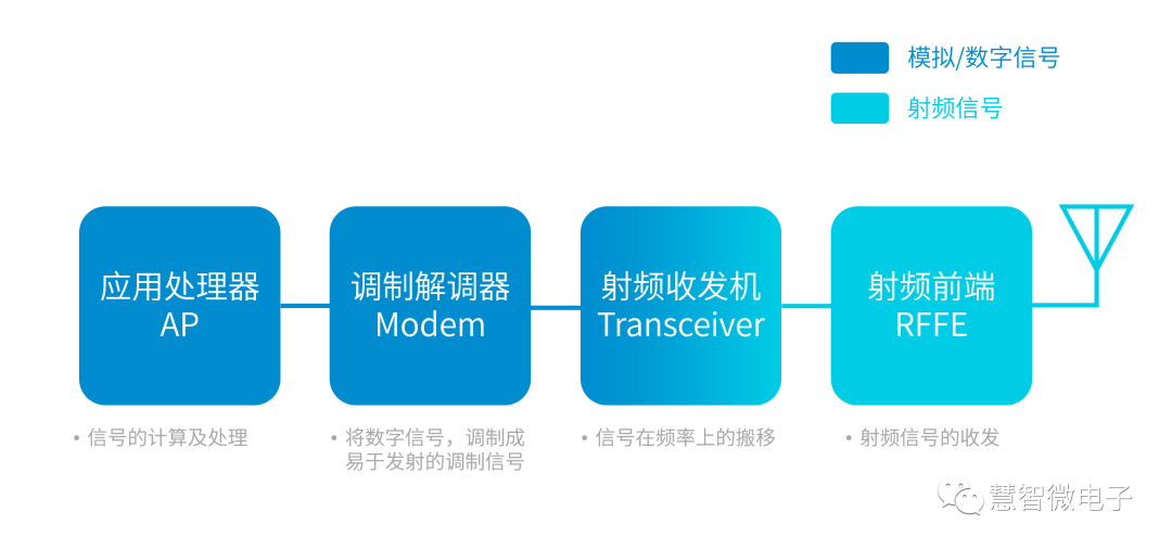
Figure: Composition of RF System
Why Perform RF Transmission
The main function of a Transceiver is to complete the transmission of analog signals to RF signals. Before understanding the Transceiver, the first question to answer is: why perform RF transmission?
RF transmission is the process of wirelessly transmitting information in the form of RF signals by utilizing the characteristics of electromagnetic waves propagating through air or other media. The frequency range of RF signals is generally from 3kHz to 300GHz.
RF transmission has several advantages:
- RF transmission can overcome the physical limitations of wired transmission, achieving long-distance, unobstructed, mobile, and flexible communication.
- RF transmission can enable multi-user and multi-scenario communication, utilizing various modulation, multiplexing, and coding techniques to improve communication efficiency and quality.
- RF transmission can achieve more complex networking, using various antenna technologies such as directional antennas, smart antennas, and phased array antennas to control and optimize the direction of signal transmission and reception.
- RF transmission can provide stronger confidentiality than wired transmission, using encryption, spread spectrum, and frequency hopping technologies to enhance communication security.
RF transmission is the foundation and core of wireless communication technology, bringing tremendous convenience and value to human society. To achieve RF transmission, an important step is to convert everyday signals such as images, sounds, and videos into RF signals. The process of converting analog signals into RF signals is the main function of RF transceivers.
Historically Significant Transceiver Circuits
Late 19th Century: The Prototype Emerges
Since Maxwell proposed the theory of electromagnetic waves in 1864, humanity has been imagining how to utilize this invisible and intangible magical entity. Around 1895, Marconi, Popov, Tesla, and others realized that electromagnetic waves could be used to achieve wireless communication and designed prototypes of radio transmitters and receivers. In 1896, Italian genius radio engineer Marconi obtained the world’s first radio patent, opening the door to the rapid development of radio communication.
In the RF conversion circuit designed by Marconi, the transmitter used a Morse code key as input, generating intermittent current pulses. The pulse signal was connected to a high-frequency oscillator, allowing Morse code to modulate the high-frequency signal, which was then transmitted into space via an antenna. In the receiver, Marconi used a metal powder detector, which could convert the wireless signal into audible sound signals, outputting them through headphones. Thus, Marconi completed the first “Transceiver” circuit in human history. This patent also became one of the important bases for Marconi to receive the Nobel Prize in Physics.
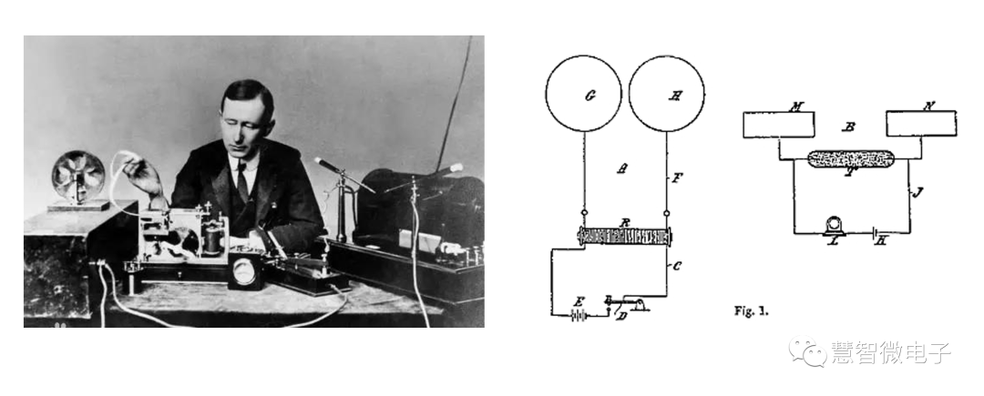 Figure: Marconi and His Designed RF Transceiver Circuit
Subsequently, Marconi improved this architecture by adding a tuning circuit, allowing the circuit’s oscillation frequency to be changed, making it easier to transmit and receive radio signals. Using his invented radio system, Marconi achieved communication across the English Channel and across the Atlantic.
If Marconi’s invention merely led humanity to experience the functionality of radio, in 1907, American engineer De Forest invented the vacuum triode, making global broadcasting, telephony, and communication possible. De Forest discovered that by adding a grid to the vacuum diode, he could control the current of the diode. Based on this characteristic, De Forest invented amplifiers, oscillators, and other circuits, enabling the amplification and oscillation of wireless signals, thus facilitating the realization of radio broadcasting and long-distance telephony.
Heterodyne and Superheterodyne: Moving Towards Modernity
The English name for the heterodyne transceiver is Heterodyne, a great invention in the history of Transceivers.
Heterodyne is a technology that creates new frequency signals by mixing two frequency signals. Two input signals are mixed through a nonlinear device (such as a vacuum tube, transistor, or diode). For example, mixing two signals with frequencies f1 and f2 produces new frequency signals of f1+f2 and f1-f2. This phenomenon is called mixing processing, and the nonlinear device used for mixing is called a mixer.
By mixing, electromagnetic waves originally propagating in space can be converted into lower frequency signals that are audible to the human ear, and with a simple detector, information reception is completed.
In 1901, Reginald Fessenden demonstrated a transceiver of this architecture. Although the triode had not yet been invented and the oscillator’s operating frequency could not be stabilized, this architecture laid a solid foundation for modern Transceivers.
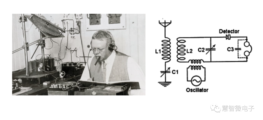 Figure: Fessenden and His Invention of the Heterodyne Receiving Circuit
After inventing this architecture, Fessenden was inspired by the Greek words “Hetero-” (different, diverse) and “dyn-” (power, capability) to name this architecture Heterodyne.
After discovering the “heterodyne” phenomenon, engineers continued to explore. They found that using higher frequency electromagnetic waves for transmission was helpful for certain application scenarios, but designing amplifiers that operate at high frequencies was extremely challenging. Engineers wondered if, since the original heterodyne idea was to shift sound frequency signals to high-frequency electromagnetic wave frequencies, could they also amplify high-frequency signals at a lower RF frequency and then shift the amplified signal to high frequency? This would eliminate the need for high-frequency, high-linearity amplifiers.
This design concept was proposed by American engineer Edwin Howard Armstrong and others in 1918. The fixed RF frequency set during the frequency shifting process is called the “Intermediate Frequency” (IF), and since this frequency exceeds the audible range, it is termed “Superheterodyne”.
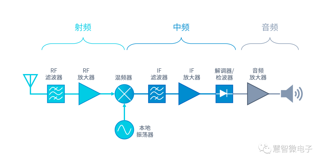 Figure: Superheterodyne Architecture
Compared to high-frequency amplifying transceivers, the superheterodyne architecture offers high sensitivity, selectivity, and stability, meeting the needs of long-distance communication for high-frequency, weak signals. Over the past 100 years, the superheterodyne structure has been widely used in wireless communication systems.
Zero Intermediate Frequency: Simplified Solutions, Increased Difficulty
The zero intermediate frequency approach does not go through the IF frequency but directly converts RF signals into baseband signals in the 0Hz frequency range. Since it is equivalent to setting the IF frequency to 0 in the superheterodyne structure, it is called the zero IF scheme (Zero IF), also known as the direct conversion scheme (Direct Conversion) and the homodyne scheme (Homodyne).
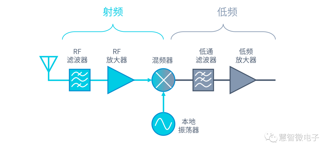 Figure: Zero Intermediate Frequency Scheme
The zero IF scheme has its unique advantages, such as:
- The zero IF scheme simplifies design, eliminating the need to shift signals to an intermediate frequency first.
- The zero IF scheme can solve the image rejection problem in the superheterodyne scheme.
- The zero IF scheme does not require intermediate frequency filters and other circuits, facilitating single-chip integration.
However, the zero IF scheme, while appearing very straightforward, brings many practical design challenges:
- Without intermediate frequency preprocessing, the baseband output level can fluctuate significantly due to variations in received signal strength.
- The local oscillator frequency being the same as the RF frequency may cause signal leakage interference.
- The mixed signal near the 0 frequency may experience DC offset.
- The local oscillator needs to have precise phase locking to accurately shift the RF frequency to near 0 frequency.
Due to these challenges, the zero IF architecture was not widely promoted after its proposal in 1924. In 1932, engineers adopted a method of comparing the local oscillator frequency with the RF frequency to correct the local oscillator frequency, allowing the local oscillator frequency to lock with the RF frequency. This circuit became the prototype of today’s Phase Locked Loop (PLL).
Other issues with zero IF were gradually resolved after the invention of the world’s first integrated circuit in 1958. The development of integrated circuits enabled PLL circuits to achieve more complex functions, and circuits with high dynamic range and high compensation characteristics could handle RF signals with large fluctuations in space. At the same time, the zero IF scheme’s suitability for single-chip integration complemented the rapid development of integrated circuits. Currently, the zero IF scheme is widely used in mobile phones, avionics, and software-defined radio systems.
From 2G to 5G: The Continuous Evolution of Transceivers
After a century of development, RF Transceivers have evolved from being able to transmit/receive a single spark to now supporting global frequency bands and complex multi-functional, multi-mode chip systems. Entering the 21st century, communication protocols continue to evolve, prompting the ongoing advancement of Transceiver technology.
2G: The Emergence of CMOS and Single-Chip Integration
The main application of the 2G cellular standard (taking GSM as an example) is voice communication, which began large-scale commercial use globally after 1990.
The popularity of 2G phones coincided with the rapid development of integrated circuits. With the evolution of Moore’s Law, by around 1995, the feature size of CMOS technology had shrunk to the 1um level. Devices with a 0.6um feature length could be used to design RF circuits at 2.4GHz, and 0.35um devices could even make 5GHz circuits possible.
However, merely having the capability to construct a single RF module was not enough to showcase the advantages of CMOS technology in RF applications; what attracted attention was its potential for large-scale single-chip integration. CMOS technology was originally prepared for digital processes and could also handle some analog circuits. If RF could also be conquered, it would enable the realization of complex mixed-signal RF circuits, all integrated on a single chip. Because of this characteristic, CMOS technology’s realization of 2G Transceivers became a research hotspot.
Implementing a fully integrated GSM Transceiver using CMOS was not straightforward; early GSM Transceivers used BJT technology and required many external components. Subsequently, some single-band GSM Transceivers designed with CMOS technology were developed, and gradually, multi-band fully integrated CMOS Transceiver chips began to emerge. The article demonstrated a fully integrated four-band GSM Transceiver designed using 0.25um CMOS technology, employing a direct conversion receiver architecture and an offset local oscillator transmitter structure, integrating PLL, VCO, mixers, intermediate frequency filters, and amplifiers, with a chip area of 3.2×3.3mm.
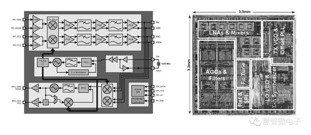 Figure: Four-Band GSM Transceiver Designed Using 0.25um CMOS Technology
3G: Simultaneous FDD Transmission and Reception, Greater Challenges for Single-Chip Integration
The communication standard represented by the 3G era is WCDMA, which is a frequency division duplex (FDD) system where the transmitter and receiver operate simultaneously at different frequencies, posing greater challenges for the design of single-chip Transceivers.
In FDD systems, the sensitivity of the receiver is affected by four factors: the noise figure of the receiver; the Rx in-band Tx noise; the Tx large signal mixing noise; and the IM2 products of the Tx signal. Among these factors, three are directly related to the isolation between the transmitter and receiver.
In the design of 3G Transceivers, methods such as enhancing LNA IIP2 and increasing notch networks can be employed to address blocking issues and improve the receiver’s performance. The article demonstrated a single-chip integrated WCDMA/HSDPA Transceiver designed using 0.18um technology, utilizing digital signal processing and tunable filters to eliminate external components, achieving a highly integrated WCDMA transceiver with high transmit-receive suppression.
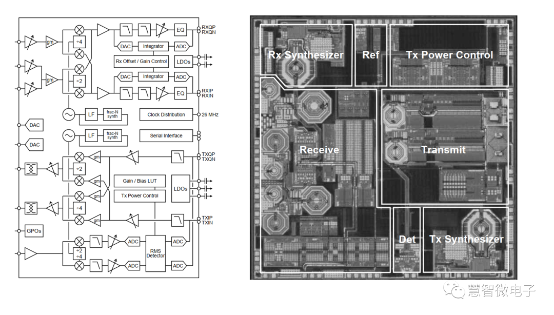 Figure: WCDMA/HSDPA Transceiver Designed Using 0.18um CMOS Technology
4G: Fragmented Frequency Bands, Increased Carrier Aggregation
4G emerged almost simultaneously with smartphones. To meet the demand for high data rate cellular communication from smartphones, more frequency bands have been opened up. Operators are also fiercely competing for frequency resources, resulting in each operator managing multiple narrow frequency bands that are non-contiguous and fragmented.
In 4G phones, the number of supported frequency bands can be as high as 40.
The increase in frequency bands poses significant challenges for Transceiver design, requiring careful consideration of sufficient reuse to keep the number of sub-modules within a reasonable range.
Another major challenge for 4G Transceivers is the support for Carrier Aggregation (CA). CA requires multiple RF paths to operate simultaneously, and the signals working together inevitably couple. In the design, it is necessary to effectively group the RF paths. As shown in the figure below, the LTE receiver system supporting 3CC has Ch1 as a 2.1GHz signal, Ch2 as a 2.3GHz signal, and Ch3 as a 700MHz signal. Since Ch1 is three times the frequency of Ch3, they need to be assigned to different mixer groups.
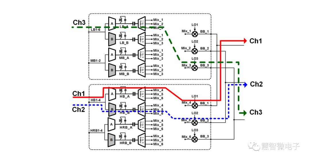 Figure: 4G LTE Transceiver Design Supporting 3CC CA
5G: MIMO/EN-DC, More Paths
The arrival of 5G has once again increased the speed of wireless communication, requiring Transceivers to achieve throughput functions of Gb/s. To this end, the 5G NR system introduces large-scale MIMO and up to 200MHz of CA. Additionally, with the demand for LTE+NR dual connectivity (EN-DC), the design difficulty of 5G NR Transceivers has significantly increased.
The article mentions that MediaTek provides a 5G Transceiver system designed using 12nm CMOS technology, which supports up to 2 inter-band uplink CAs, 6 inter-band downlink CAs, and supports 4×4 MIMO, as well as NR 200MHz CA. To achieve these functions, the Transceiver integrates 20 Rx paths, covering frequency bands from 600MHz to 6GHz. Even with internal LNA multiplexing technology, the internal LNA still reaches 28. The Transceiver also employs a large number of digital circuits to support a bandwidth of 200MHz. Under NR 200MHz/4×4 MIMO/256QAM, it can achieve a throughput of 5Gb/s.
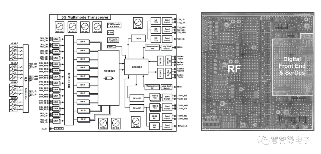
Figure: 5G Transceiver Designed Using 12nm CMOS Technology
Conclusion
As protocols evolve, the communication capabilities required of terminals are increasing, with RF Transceiver functions evolving from merely receiving and transmitting a spark to now needing to transmit data volumes of several Gb per second. These demands pose significant challenges for Transceiver design.
The development of CMOS RF integrated circuits has made all of this possible. Based on the continuously evolving CMOS technology, different circuit modules can be integrated on a single chip, achieving integration of multiple frequency bands, multiple modes, and even multiple channels, allowing the incredibly complex RF transceiver functions to be integrated into a compact space.
The complex implementation of Transceivers has also raised the bar for Transceiver design. In the early 3G era, there were multiple third-party companies designing RF Transceivers, but by the time of 5G, the RF Transceivers for mobile terminals have been monopolized by leading SoC platform companies such as Qualcomm and MediaTek.
As the complexity of Transceiver functions increases, higher requirements are also placed on the use of Transceivers and the coordination with other circuits in the RF front-end. In the latest 5G Transceiver user manuals from Qualcomm and MediaTek, in addition to introducing basic performance, a significant portion is dedicated to discussing the precautions for using Transceivers under CA and EN-DC, as well as the considerations needed when coordinating with the RF front-end.
In the future, RF Transceivers will face demands for more frequency bands, higher bandwidth, lower power consumption, and higher integration levels. To meet these requirements, RF Transceivers may adopt more advanced processes, more flexible architectures, and smarter control technologies, while also placing higher demands on the applications and usage of Transceivers.References:
[1]. GUGLIELMO MARCONI, Patent 5028, March 5, 1896, http://www.alternativaverde.it/sttlcing/documenti/Marconi/1896/marc05031896.htm
[2]. A. A. Abidi, “The future of CMOS wireless transceivers,” in IEEE International Solid-State Circuits Conference. Digest of Technical Papers (ISSCC), San Francisco, CA, USA, 1997, pp. 118-119.
[3]. B. Razavi, “Challenges in portable RF transceiver design,” in IEEE Circuits and Devices Magazine, vol. 12,1996
[4]. T. D. Stetzler, I. G. Post, J. H. Havens, and M. Koyama, “A 2.7–4.5 V single chip GSM transceiver RF integrated circuit,” IEEE J. Solid-State Circuits, vol. 30, no. 12, pp. 1421–1429, Dec. 1995
[5]. P. Orsatti, F. Piazza, and Q. Huang, “A 20-mA-receive, 55-mA-transmit, single-chip GSM transceiver in 0.25-um CMOS,” IEEE J. Solid-State Circuits, vol. 34, no. 12, pp. 1869–1880, Dec. 1999.
[6]. M. S. J. Steyaert, J. Janssens, B. De Muer, M. Borremans, and N. Itoh, “A 2-V CMOS cellular transceiver front-end,” IEEE J. Solid-State Circuits, vol. 35, no. 12, pp. 1895–1907, Dec. 2000.
[7]. E. Song, Y. Koo, Y.-J. Jung, D.-H. Lee, S. Chu and S.-I. Chae, “A 0.25-μm CMOS quad-band GSM RF transceiver using an efficient LO frequency plan,” IEEE Journal of Solid-State Circuits, vol. 40, no. 5, pp. 1094-1106, May 2005.
[8]. B. Tenbroek, J. Strange, D. Nalbantis, M. Poulton and A. Burrows, “Single-chip tri-band WCDMA/HSDPA transceiver without external SAW filters and with integrated TX power control,” in IEEE International Solid-State Circuits Conference – Digest of Technical Papers (ISSCC), San Francisco, CA, USA, 2008, pp. 480-481.
[9]. Menzel, W., & Lee, K. (2015). A Rel-12 2G/3G/LTE-Advanced 3CC Cellular Receiver. IEEE Journal of Solid-State Circuits, 50(1), 54-68.
[10]. Ming-Da Tsai et al., “A 12nm CMOS RF Transceiver Supporting 4G/5G UL MIMO,” 2020 IEEE International Solid-State Circuits Conference (ISSCC), San Francisco, CA, USA, 2020, pp. 180-182, doi: 10.1109/ISSCC19947.2020.9062939.
This content is reproduced only to represent the author’s views
It does not represent the position of the Institute of Semiconductors, Chinese Academy of Sciences
Editor: Qian Niao