
Click the blue text above to follow us.
The core challenge of mixed signal PCB design lies in how to allow analog circuits and digital circuits to coexist on the same board while minimizing signal interference.
Whether it is the weak analog signals collected by sensors or the high-frequency switching digital signals from processors, improper layout can lead to issues such as noise coupling and signal integrity degradation, ultimately resulting in subpar system performance.
Mixed signal PCB layout is not a simple process of “placing components and then routing”; it requires planning from the source. The board layers determine the signal return paths, the ground plane ensures noise isolation, and power and decoupling techniques safeguard system stability.
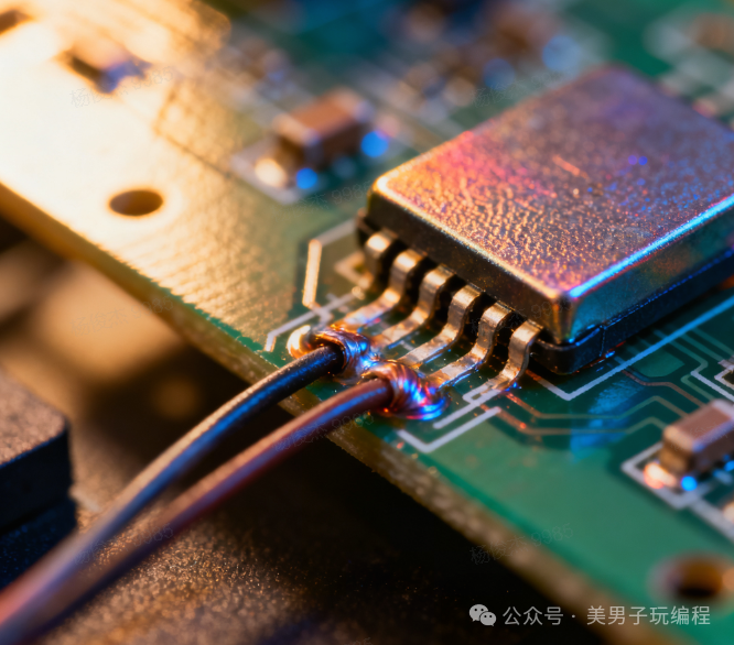
This article will unfold step by step according to the design process, using plain technical language and clear practical rules to help readers establish a systematic layout mindset.
1
Component Placement: The “Foundation Engineering” of Layout Design
Component placement is the first step in mixed signal PCB design, akin to the floor planning before building a house, directly determining the subsequent routing difficulty and the system’s ability to resist interference.
The core principle is to “partition by module and layout by signal path,” avoiding interference from high-noise components on sensitive circuits while reserving reasonable space for subsequent routing.
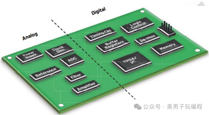
Overall Layout Logic
Before layout, it is necessary to sort out the circuit modules: separate and classify analog modules (such as sensors, amplifiers, ADC/DAC), digital modules (such as MCU, FPGA, clock circuits), and power modules (such as LDO, DC-DC), ensuring that components of the same function are “concentrated nearby.”
For example, sensors and amplifiers should be placed close together to reduce the analog signal transmission path; processors and memory chips should be arranged around the “shortest signal path” to avoid high-frequency signal delays.
At the same time, routing channels should be planned in advance: reserve at least 2-3mm of routing space around core chips (such as MCUs), avoid crossing analog signal paths with digital signals, and reserve wide routing space for high current power paths (usually ≥1mm).
Key Component Placement Rules
(1) Connectors: Prioritize positioning, place near the edge
All connectors (such as USB, sensor interfaces) should be prioritized for placement at the PCB edge, facilitating external device connection and avoiding occupation of the core area of the board.
When placing, note that ESD protection components (such as TVS diodes) must be close to the connector pins, within ≤5mm, to ensure rapid discharge of static electricity; if the connector transmits both analog and digital signals (such as interfaces with sampling functions), a “transition zone” should be defined near the connector to avoid direct signal crossing.
(2) Heat-sensitive components: Keep away from heat sources, separate zones
Heat-sensitive components such as oscillators and sensors must maintain a distance of at least 3cm from power devices (such as MOSFETs, DC-DC chips) to avoid parameter drift (such as oscillator frequency shift) caused by temperature rise during operation.
For example, the 11.0592MHz oscillator of the 51 microcontroller may experience increased serial communication error rates if placed near a heat-generating linear regulator.
(3) Mixed signal devices: Stand at the “boundary of analog and digital”
ADC/DAC are typical mixed signal devices and should be placed at the junction of the analog and digital areas—analog pins (such as AIN, AVDD, AGND) facing the analog area, and digital pins (such as DOUT, DVDD, DGND) facing the digital area to avoid noise coupling caused by pin crossing.
For example, the 12-bit ADC chip ADS1115 should have its analog input terminal placed close to the amplifier output, while the digital output terminal should be near the MCU’s SPI interface, with a distance controlled within 20mm to reduce signal transmission loss.
Isolation Strategy for Analog and Digital Modules
Analog circuits are extremely sensitive to noise (such as microvolt-level sensor signals), while digital circuits generate high-frequency switching noise (such as MCU IO port switching), so physical isolation must be implemented on the PCB:
-
Partitioning: It is recommended to concentrate the analog area on the left side of the PCB, the digital area on the right side, with a reserved isolation zone of ≥10mm in between (if the digital circuit frequency is ≥100MHz, the isolation zone should be expanded to 15mm);
-
Component allocation: Sensitive components such as amplifiers, reference voltage sources (such as REF3030), and low-noise LDOs must be placed in the analog area; high-noise components such as clock generators, logic gates, and high-speed interface chips must all be allocated to the digital area;
-
Cross-zone prohibitions: Digital signal lines are prohibited from entering the analog area, and analog signal lines must not enter the digital area. If crossing is necessary (such as the digital output line of an ADC), a complete ground plane must be reserved below the crossing point to reduce coupling.
Decoupling Capacitors and Oscillator “Close Layout”
(1) Decoupling capacitors: Follow closely behind power pins, “the smaller the closer”
The core function of decoupling capacitors is to provide instantaneous current to the chip and suppress power noise, so they must be “close to the chip power pins”:
-
Small value capacitors (0.01μF-0.1μF, ceramic material) should be within ≤3mm of the pins, preferably using 0402 package to reduce trace inductance;
-
Large value capacitors (10μF-100μF, electrolytic or tantalum capacitors) should be within ≤25mm (about 1 inch) of the pins to filter out low-frequency noise;
-
If the chip has multiple power pins (such as the core voltage and IO voltage of an FPGA), each pin must be configured with a separate decoupling capacitor and cannot be shared.
(2) Oscillator: Independent area, away from sensitive circuits
Oscillators are high-frequency noise sources (for example, the harmonics of an 8MHz oscillator may reach several hundred MHz), so care must be taken during layout:
-
The distance between the oscillator and the chip’s clock pin should be ≤10mm, and the load capacitors (such as 22pF) should be placed close to both ends of the oscillator, with trace length differences ≤1mm to avoid frequency shifts;
-
Analog components (such as amplifiers, ADCs) are prohibited from being placed within a 300mil (approximately 7.62mm) range around the oscillator, and the PCB layers below (including top, bottom, and inner layers) must be completely grounded, prohibiting any signal traces;
-
If there are multiple oscillators on the board (such as the MCU oscillator and RF oscillator), the distance between them should be ≥20mm to avoid harmonic interference.
2
Power Module Design: The “Energy Guarantee” for System Stability
The power supply is the “heart” of the mixed signal system. If power noise enters the analog circuit, it may directly lead to signal distortion; if the digital power supply’s transient response is insufficient, it can cause the processor to crash.
The core of power module design is “isolation, proximity, and low impedance,” meaning that analog and digital power supplies must be separated, the power module should be close to the load, and the routing should be short and wide.
Isolation Design of Power Modules
Analog and digital power supplies must be powered independently, even if the input voltage is the same (such as both being 3.3V), they must be designed separately:
-
Power entry: If sharing an external power supply, it is necessary to separate at the entry point using a ferrite bead (such as 100Ω/100MHz) or a 0Ω resistor, with the analog side connected to an LDO (such as AMS1117) and the digital side connected to a DC-DC (such as MP1584) to avoid the switching noise of the digital power supply coupling into the analog side;
-
Power planes: In multi-layer PCBs, the analog power plane (such as AVDD) and the digital power plane (such as DVDD) must be physically separated, with boundaries aligned with the analog/digital areas, and the copper foil thickness of the planes should be ≥35μm (1oz) to ensure low impedance (<50mΩ);
-
Load matching: The power path for high current digital loads (such as the core voltage of an FPGA) must be planned separately, with a line width ≥2mm (carrying 2A), away from the analog power plane to avoid voltage fluctuations caused by current changes.
The “Short, Straight, and Wide” Principle of Power Routing
The key to power routing is to reduce inductance and resistance:
-
Short: The distance from the power module to the load should be ≤50mm, for example, the routing from the LDO output to the ADC’s AVDD pin should be as short as possible to minimize noise loss;
-
Straight: Avoid zigzag or winding routes; if a turn is necessary, use a 45° angle or arc transition to reduce signal reflection;
-
Wide: Determine the line width based on the current size; for example, a 1A current requires a line width of ≥1mm, and 2A requires ≥2mm. High current paths (such as DC-DC outputs) can use copper filling to further reduce impedance.
Special Optimization of Power for ADC/DAC
The power noise of ADC/DAC directly affects conversion accuracy (1mV noise can cause a 12-bit ADC to produce a 0.5LSB error) and requires additional optimization:
-
Analog power (AVDD): Should be drawn separately from an LDO, not sharing paths with other analog components, with a 10-100Ω ferrite bead in series (select based on noise frequency, such as 100Ω for 100MHz noise);
-
Reference voltage (VREF): Should be routed with the thickest (≥0.3mm) and shortest (<10mm) traces, away from digital lines and DC-DC, with dedicated filtering capacitors (100nF ceramic + 10μF tantalum) placed close to the VREF pin, grounding only connected to AGND;
-
Power filtering: At the power pins of the ADC/DAC, use “100nF + 1μF” ceramic capacitors in parallel, with the capacitor’s ground directly connected to the ground plane to reduce ground inductance.
3
Decoupling Techniques: The “Noise Filter” for Power Integrity
The essence of decoupling techniques is to provide a “discharge channel” for power noise, ensuring stable voltage at the chip power pins.
To effectively decouple, one must first understand the Power Supply Rejection Ratio (PSRR)—this parameter measures the chip’s resistance to power noise; the higher the PSRR, the less the chip is affected by power noise.
However, in practical applications, PSRR decreases with increasing frequency (for example, the PSRR of the high-performance amplifier OP1177 is 120dB at 1kHz and drops to 60dB at 1MHz), so decoupling capacitors must be used to suppress high-frequency noise.
Selection and Combination of Decoupling Capacitors
Different capacitors filter different frequency bands and must be used in combination to cover a wide frequency range:
-
Low-frequency decoupling (<1kHz): Use 10μF-100μF electrolytic or tantalum capacitors as a “charge reservoir” for transient currents, reducing power voltage fluctuations;
-
Mid-frequency decoupling (1kHz-100MHz): Use 1μF-10μF ceramic capacitors (X7R material, good temperature stability) to filter out switching noise on the power line;
-
High-frequency decoupling (>100MHz): Use 0.01μF-0.1μF ceramic capacitors (C0G material, excellent high-frequency characteristics), placed close to the chip power pins to suppress high-frequency harmonics.
For example, next to the power pins of an MCU, it is common to pair a “10μF tantalum capacitor + 0.1μF ceramic capacitor,” where the former addresses transient currents such as motor startups, and the latter filters out high-frequency noise generated by IO port switching.
Key Points for Decoupling Capacitor Layout
The effectiveness of decoupling capacitors depends 80% on their placement; the core rule is “shortest path, low inductance connection”:
-
Close to the pins: Small value capacitors (such as 0.1μF) should be within ≤3mm of the chip power pins, and large value capacitors (such as 10μF) should be ≤25mm to avoid long traces introducing inductance;
-
Ground priority: The ground terminal of the capacitor should be directly connected to the ground plane, preferably through a “T-connection” or via directly to the ground plane, without routing through other components;
-
Avoid sharing: Each chip’s decoupling capacitor should be configured independently, and multiple chips should not share a set of capacitors, especially analog and digital chips, which need separate decoupling.
Decoupling Solutions for Special Scenarios
If the board has strong noise sources (such as RF modules or high-power motor drives), additional measures should be taken on top of basic decoupling:
-
Power entry: Add a π filter (inductor + two capacitors), with inductor values of 10-100μH and capacitors of 10μF + 0.1μF to suppress external noise from entering;
-
High-frequency noise isolation: Place ferrite beads (such as BLM18PG102SN1) in series on the analog power line, with bead impedance ≥100Ω at noise frequencies to block high-frequency noise from entering the analog circuit;
-
Large area copper filling: Fill unused PCB areas with ground copper, connecting to the ground terminal of decoupling capacitors to form a “noise absorption zone” and reduce EMI radiation.
4
PCB Layer Design: The “Channel Planning” for Signal Return
After completing component placement, the number of PCB layers and layer structure must be determined before routing—the layer structure determines the signal return paths, and improper design may lead to increased ground impedance and aggravated signal crosstalk.
For mixed signal PCBs, a four-layer board is the most cost-effective choice, meeting isolation needs without excessively increasing costs; if the system complexity is high (such as multiple ADCs or high-frequency digital circuits), it should be upgraded to a six-layer board.
Typical Four-Layer Board Structure Design
The classic structure of a four-layer board is “Signal – Ground – Power – Signal,” with clear functions for each layer and strong anti-interference capability, configured as follows:
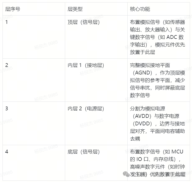
The advantage of this structure is that the ground layer is adjacent to the power layer, forming a natural “plane capacitor” (under FR4 material, a plane capacitor with a spacing of 4-6mil is about 75pF/square inch), which can assist in filtering high-frequency power noise; the top layer analog signals reference the ground layer, while the bottom layer digital signals reference the power layer, with both isolated by the ground layer to reduce cross-interference.
Key Considerations for Layer Design
-
Plane Integrity: The ground layer and power layer should be kept as complete as possible, avoiding large areas of cutouts (such as cutting the plane to avoid vias), especially for the analog ground layer, as breaks can lead to increased ground impedance and ineffective noise dissipation;
-
Layer Alignment: The boundaries of the power layer must align with the analog/digital partition of the ground layer; for example, the analog power area must be directly below the analog ground layer to avoid noise coupling caused by “power-ground” crossing;
-
Via Connections: The ground plane of multi-layer boards must be connected through a “via array” (such as one ground via every 20mm) to ensure consistent ground impedance across layers, allowing high-frequency noise to dissipate across layers.
5
Ground Plane Design: The “Core Defense Line” for Noise Isolation
Grounding is the most error-prone aspect of mixed signal PCB design and is a key factor affecting system performance.
Many junior engineers fall into the misconception that “analog ground and digital ground must be separated”; in reality, the design of the ground plane should be chosen based on system complexity—simple systems benefit from a single ground plane, while complex systems require separation, with the core goal being “to provide all return currents with low impedance paths without interfering with sensitive circuits.”
Single Ground Plane: The Preferred Choice for Simple Systems
If the system contains only 1-2 low current ADC/DACs (such as 8-bit ADCs with currents <10mA), a single complete ground plane is the best choice, with advantages including:
-
Low Impedance: A complete copper ground plane has far lower ground impedance than a split plane, allowing return currents to flow along the shortest path and reducing ground bounce noise;
-
Easy Routing: There is no need to consider plane split boundaries, allowing signal lines to be freely planned and reducing design difficulty;
-
Anti-Interference: A complete ground plane can shield external EMI while reducing internal signal radiation.
-
Design Points:
-
Partition Planning: Use component layout to divide the “analog area” and “digital area” on the ground plane, keeping the ground copper foil under analog components intact, ensuring that the return current of digital components does not flow through the analog area;
-
Signal Control: Digital signal lines should only be routed in the digital area, and analog signal lines should only be routed in the analog area to avoid lengthening return current paths due to crossing;
-
Single Point Grounding: The power ground, analog ground, and digital ground should connect at a single point at the power entry (such as through a 0Ω resistor) to ensure consistent grounding potential across the system.
Separation of Analog Ground and Digital Ground: Solutions for Complex Systems
When the system contains multiple high current ADC/DACs (such as 16-bit ADCs with currents >50mA) or high-frequency digital circuits (such as clocks above 100MHz), a single ground plane may not effectively isolate noise, requiring the use of separate ground planes:
-
Plane Segmentation: Physically separate AGND and DGND in the ground layer, with a gap of ≥1mm, aligning the split boundary with the analog/digital areas;
-
Single Point Connection: AGND and DGND should only connect at one point, preferably below the ADC/DAC or at the power entry, using a ferrite bead (100Ω/100MHz) or a 0Ω resistor to connect, avoiding the formation of loop currents;
-
Component Allocation: The ground pins of analog components (amplifiers, sensors) should only connect to AGND, while digital components (MCUs, logic gates) should only connect to DGND. The AGND pins of mixed signal components (ADC/DAC) connect to the AGND plane, and the DGND pins connect to the DGND plane, with internal single point connections.
For example, in a multi-channel data acquisition card, the AGND of four 16-bit ADCs should all connect to the AGND plane, while the DGND of the FPGA connects to the DGND plane, with both connected at the power entry through a 0Ω resistor to isolate digital noise while ensuring consistent grounding potential.
Ground Design Checklist
Regardless of the grounding scheme used, after layout completion, the following checklist should be verified:
- Are all chip ground pins directly connected to the corresponding ground plane, with no long traces (≤5mm)?
- Is the ground plane complete, with no large areas of breakage (especially under the analog area)?
- Do digital signal lines cross the split boundary between AGND and DGND (prohibited crossing, otherwise return current paths will be discontinuous)?
- Are the AGND and DGND of mixed signal components (ADC/DAC) connected according to the datasheet requirements, with no misconnection?
- Are there sufficient ground vias, and is the ground plane of multi-layer boards connected through a via array (at least one via every 20mm)?
- Is the unused PCB area grounded and connected to the corresponding ground plane, with no floating copper?
Mixed signal PCB layout design is a combination of “rules + experience”—mastering the partition logic of component placement, frequency matching of power decoupling, path planning of PCB layers, and isolation techniques of ground planes can help avoid 80% of common problems.
For junior engineers, there is no need to pursue complex optimization schemes; first, implement the basic principles:
-
Component Placement: Analog and digital partitioning, sensitive components away from noise sources;
-
Power Design: Separate analog and digital power supplies, with short, straight, and wide routing;
-
Decoupling Capacitors: Close to pins, with high and low frequency combinations;
-
PCB Layers: Prefer four-layer boards with “Signal – Ground – Power – Signal”;
-
Ground Plane: Use a single plane for simple systems, and single-point separation for complex systems.
In practical design, the guidelines in this article can be gradually verified: first plan module partitions, then place key components, followed by determining layer structures, and finally optimizing routing and grounding.
When encountering noise issues, first check if the grounding is complete and if the decoupling capacitors are in place—most of the time, optimizing these basic aspects can significantly improve system performance.
As design experience accumulates, further learning about high-frequency signal integrity, EMC optimization, and other advanced knowledge can be pursued, but solid foundational layout skills remain the core competitiveness of mixed signal PCB design.

 Click Read the Original for more exciting content~