In the field of printed circuit board (PCB) manufacturing, graphic transfer is one of the core processes. As electronic devices trend towards lightweight and miniaturization, the precision requirements for PCB traces are increasing, and traditional exposure technologies are struggling to meet the demands of modern electronic manufacturing.
Laser Direct Imaging (LDI) technology has emerged as a key technology for high-precision PCB manufacturing.
01 Technology Overview: Understanding LDI Technology
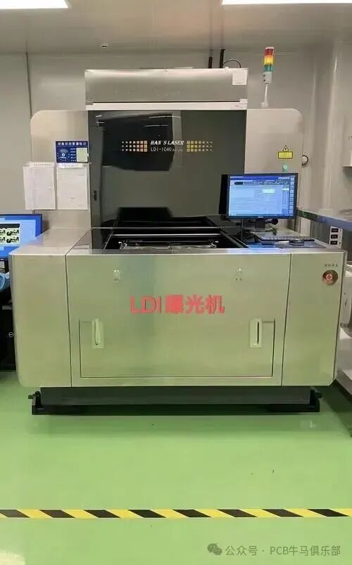
LDI stands for Laser Direct Imaging, which is a technology that uses the principle of laser direct imaging to project circuit images directly onto a substrate coated with photoresist in the form of a laser beam, thereby achieving graphic transfer.
Since Excellon launched the first argon laser imaging device, direct imaging technology has developed for over 40 years. The initially commercially successful digital processes all utilized laser technology, while recent technologies have begun to adopt non-laser light sources such as light-emitting diodes.
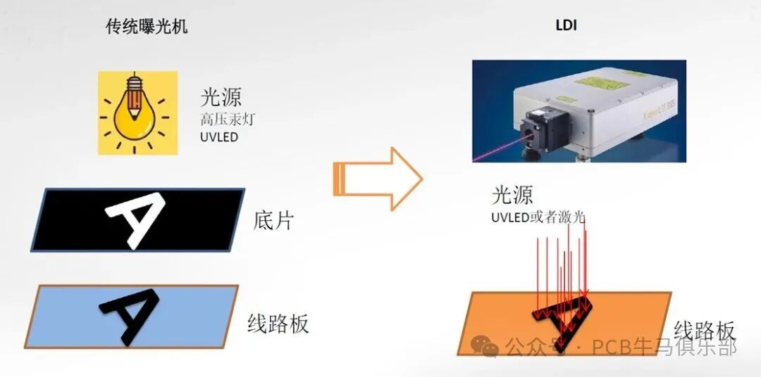
Unlike traditional exposure technologies that require physical photomasks, LDI technology does not need a physical mask and directly forms circuit patterns on the photoresist using a laser beam.
This not only eliminates the process of manufacturing and adjusting film but also significantly improves the precision and alignment capability of graphic transfer.
02 Working Principle: How Laser Direct Imaging Works
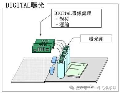
The working process of the LDI laser direct imaging system is quite precise, with its core utilizing digital graphic data to control the laser beam for direct exposure on a substrate coated with photosensitive material.
The system first receives CAD data from the design department and then directs the laser beam to the surface of the substrate through a precision optical system.
Laser scanning systems often use polygon mirrors or micro-mirror arrays (such as TI’s DMD devices) to control the direction of the laser beam.
During the imaging process, low-power laser beams are generated by one or more laser diodes, with a wavelength of approximately 405nm.
These laser beams pass through a complex optical path and are precisely exposed on the surface of the photoresist-coated board in the form of pixel points.
The alignment system is one of the key components of LDI equipment. In a vacuum environment, markers placed on the operating table begin to image the target points or holes on the bottom of the panel.
A CCD camera then aligns the incoming panel with the operating table, and after flipping the panel, the same operation is repeated on the top of the panel.
This high-precision alignment mechanism allows LDI to achieve nearly perfect inter-layer alignment, which is crucial for the production of high-layer-count, high-density interconnect boards.
03 Advantages Comparison: Differences Between LDI and Traditional Exposure Technologies
Exposure Method
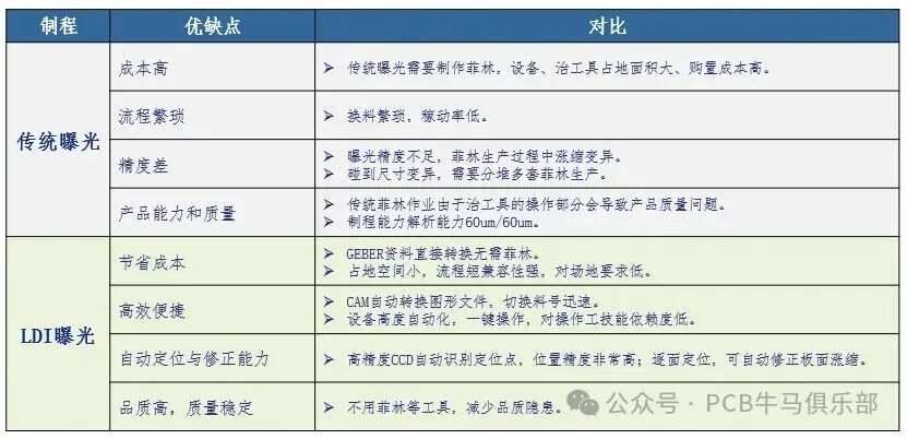
Compared to traditional exposure technologies, the most significant feature of LDI is that it does not use film, which is referred to as “electronic film” for direct laser imaging.
Traditional film usage presents several issues: poor dimensional stability, susceptibility to deformation; limited usage of films; and the need to replace films and adjust alignment, which is quite time-consuming.
In actual production, it is quite common to change 30-40 sets of films in a 20-hour operation; if each change takes 10 minutes, the time consumed would be 300-400 minutes, which translates to 5-6.5 hours of the workday.
In contrast, the LDI system typically requires only a few seconds to change the circuit.
Alignment Capability
In terms of alignment precision, the advantages of the LDI system are even more pronounced.
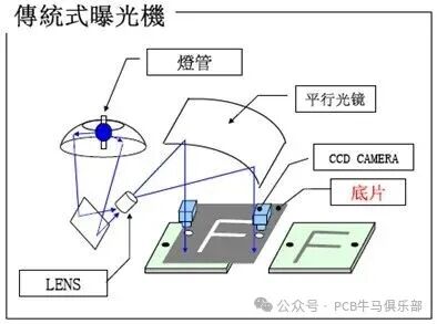
Traditional exposure machines rely on manual alignment and physical films, which limits alignment precision, especially in high-layer-count, high-density, and buried blind hole components.
LDI, on the other hand, uses a vision system to automatically identify targets and precisely calibrate through computer algorithms, compensating for errors caused by material deformation to achieve micron-level alignment precision.
Resolution Capability
With LDI exposure technology, the minimum line width/spacing can achieve 1.8/1.8MIL.
In contrast, traditional parallel exposure machines struggle to achieve such fine line resolution due to diffraction effects of light and the angle of emission from the lamps.
Cost-Effectiveness
Although the initial investment in LDI equipment is relatively high, in the long run, it eliminates the costs of film production, maintenance, and storage, reduces material waste and rework rates, thus providing significant cost advantages in small-batch, multi-variety production scenarios.
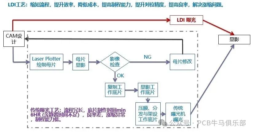 Limitations of Traditional Exposure Methods: 1. Due to uneven illumination, the repeatability of line width near the edges is poor. 2. Films can expand and contract, leading to alignment precision issues, with errors reaching several hundred microns on a 500mm board. High precision requirements result in low yield and quality. Advantages of LDI Exposure Methods: 1. Shortened cycle (reducing film processes for direct imaging) 2. Improved quality (non-contact, uniform energy, high alignment precision) 3. Cost savings (no need for film, utilizing virtual electronic film, improved quality)04 Key Control Points: Ensuring LDI Imaging Quality
To ensure LDI imaging quality, it is essential to strictly control the following key points:
Laser energy control is the core of the LDI process. The stability of laser energy directly affects exposure results and line width precision.
Insufficient energy can lead to underexposure of the photoresist, resulting in incomplete graphics; excessive energy may cause line width deviations or even damage the material.
Regular calibration of laser power is necessary to ensure energy output remains stable within the process window.
Precise alignment is another key aspect of LDI technology. The LDI system uses high-resolution CCD cameras to capture alignment markers on the board surface, calculating scaling, rotation, and displacement parameters through algorithms to achieve precise graphic alignment.
For warped substrates, the system must also have three-dimensional surface compensation capabilities to ensure uniform focus across different locations.
Environmental control is equally important. Variations in temperature and humidity can affect material dimensional stability, thereby impacting imaging precision.
The LDI working environment should maintain constant temperature and humidity, with temperature controlled at 22±2°C and relative humidity kept between 50-60%.
Material compatibility is a commonly overlooked but crucial factor. LDI requires the use of specialized LDI-type dry films and LDI-type inks, which are highly sensitive to the specific wavelengths (such as 405nm) used in LDI.
05 Specialized Materials: Requirements for LDI-Type Dry Films and Inks
With the popularization of LDI technology, the development of specialized materials has become increasingly important. Unlike traditional UV exposure, LDI uses high-energy, single-wavelength laser sources, which requires that the photosensitive materials must match the laser wavelength.
LDI-specific dry films need to possess characteristics such as high sensitivity, high resolution, and high adhesion.
The FD series developed by leading companies is a new type of water-soluble dry film specifically designed for laser direct imaging, featuring high sensitivity, high resolution, high adhesion, and quick film removal.
The digital photoresist materials developed by the Industrial Technology Research Institute focus on the photosensitive wavelength of 403 nm and high resolution.
They have introduced functional groups suitable for the DLT photosensitive wavelength in the design of high-sensitivity photosensitizers, controlling the light absorption wavelength while developing new synthesis technologies for photosensitive resins and photoresist formulations to improve the sensitivity and resolution of photoresist materials.
LDI-specific solder mask inks also need to be optimized to adapt to laser exposure. Compared to traditional solder mask inks, LDI-type inks should have higher absorption efficiency at the laser wavelength while maintaining excellent developability and chemical resistance.
Materials developed by the Industrial Technology Research Institute can achieve a line width of 2.5 μm after development under exposure doses of <20 mJ/cm², with a line width variation of less than 5%.
The development of these specialized materials enables LDI technology to maximize its effectiveness in PCB trace formation and solder mask patterning, meeting the manufacturing needs of fine traces and small-pitch electronic products.
 Note: The above discussion is for reference only and serves as a starting point for further exploration! Each factory’s chemicals/processes/equipment/product structures, etc., have various differences, and one must not rigidly apply these experiences; all effective improvement measures must be based on experimental data! As a professional quality of engineering technicians, it is essential to “speak with data.”
This public account will continue to update information related to PCB manufacturing and cutting-edge technologies.
Thank you, not only for being so good-looking and handsome but also for being able to move your golden fingers to make money, please follow + collect + like + share + comment!!! Follow to avoid getting lost!!!
Original content is not easy; if you want to reprint, please private message the author, obtain consent, and indicate the source before reprinting. Thank you for your cooperation!