In PCB design, as the frequency rapidly increases, various interferences that differ from low-frequency PCB designs will arise. Moreover, as the contradiction between increasing frequency and the miniaturization and cost reduction of PCBs becomes more pronounced, these interferences are becoming more numerous and complex. In our practical research, we have summarized four main types of interference: power noise, transmission line interference, coupling, and electromagnetic interference (EMI). By analyzing various interference issues in high-frequency PCBs and combining them with practical work, effective solutions have been proposed.
1. Power Noise
In high-frequency circuits, the noise carried by the power supply has a particularly significant impact on high-frequency signals. Therefore, the first requirement is that the power supply must be low-noise. Here, clean ground and clean power are equally important. Why is that? The characteristics of the power supply are shown in Figure 1. It is evident that the power supply has a certain impedance, which is distributed across the entire power supply, and thus, noise will also superimpose on the power supply. Therefore, we should minimize the impedance of the power supply as much as possible, so it is best to have dedicated power and ground layers. In high-frequency circuit design, power is designed in the form of layers, which is generally much better than designing it in the form of a bus, allowing the return path to always follow the path of least impedance. Additionally, the power board must provide a signal return path for all signals generated and received on the PCB, minimizing the signal return path and thus reducing noise, which is often overlooked by low-frequency circuit designers.
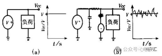
Figure 1 Power Supply Characteristics
Methods to eliminate power noise in PCB design include the following:
1. Pay attention to vias on the board: Vias require openings to be etched on the power layer to allow space for the vias to pass through. If the openings on the power layer are too large, they will inevitably affect the signal return path, forcing the signal to detour, increasing the loop area and noise. At the same time, if some signal lines are concentrated near the openings, sharing this segment of the return path, the common impedance will cause crosstalk, as shown in Figure 2.
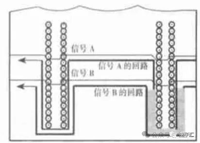
Figure 2 Common Path of Bypass Signal Return
2. Ensure sufficient ground connections for the wires: Each signal needs its own dedicated signal return path, and the loop area of the signal and return path should be as small as possible, meaning the signal and return path should run in parallel.
3. Separate analog and digital power supplies: High-frequency devices are generally very sensitive to digital noise, so the two should be separated. They can be connected together at the power entry point. If a signal needs to cross between the analog and digital sections, a loop can be placed at the crossing to minimize the loop area. The crossing for signal return between analog and digital is shown in Figure 3.
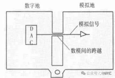
Figure 3 Crossing for Signal Return between Analog and Digital
4. Avoid overlapping separate power supplies across different layers: Otherwise, circuit noise can easily couple through parasitic capacitance.
5. Isolate sensitive components: such as PLLs.
6. Place power lines: To reduce the signal return path, place power lines next to signal lines to reduce noise, as shown in Figure 4.
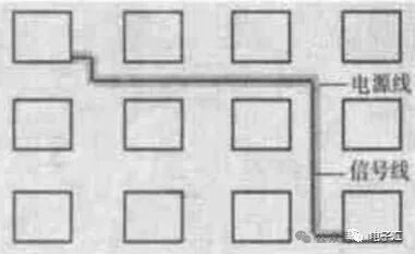
Figure 4 Placing Power Lines Next to Signal Lines
2. Transmission Lines
There are only two types of transmission lines that can occur in PCBs: strip lines and microstrip lines. The biggest problem with transmission lines is reflection, which can cause many issues, such as the load signal being a superposition of the original signal and the echo signal, increasing the difficulty of signal analysis; reflection can cause return loss, which has an impact on the signal as serious as additive noise interference:
1. Signal reflection back to the signal source increases system noise, making it more difficult for the receiver to distinguish between noise and signal;
2. Any reflected signal will generally degrade signal quality and alter the shape of the input signal. The main principle for solving this is impedance matching (for example, interconnect impedance should closely match the system impedance), but sometimes impedance calculations can be complicated, and some transmission line impedance calculation software can be referenced.Methods to eliminate transmission line interference in PCB design include:
(a) Avoid discontinuities in transmission line impedance. Discontinuities in impedance occur at points of abrupt changes in the transmission line, such as sharp corners and vias, which should be avoided as much as possible. Methods include: avoiding sharp corners in routing, using 45° angles or curves whenever possible; minimizing the use of vias, as each via is a point of impedance discontinuity, as shown in Figure 5; avoid outer layer signals passing through inner layers, and vice versa.
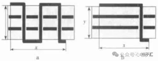
Figure 5 Methods to Eliminate Transmission Line Interference
(b) Do not use stubs. Any stub is a source of noise. If the stub is short, it can be terminated at the end of the transmission line; if the stub is long, it will act as a source of large reflections, complicating the problem, so it is recommended not to use them.
3. Coupling
1. Common impedance coupling: This is a common coupling channel where the interference source and the affected device often share certain conductors (such as return power, buses, common ground, etc.), as shown in Figure 6.
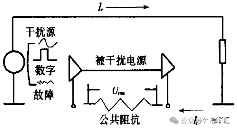
Figure 6 Common Impedance Coupling
In this channel, the drop in Ic can cause common-mode voltage in the series current loop, affecting the receiver.
2. Field common-mode coupling can cause radiation sources to generate common-mode voltage on the loop formed by the affected circuit and the common reference plane. If the magnetic field predominates, the common-mode voltage generated in the series loop is Vcm=-(△B/△t)*area (where △B is the change in magnetic induction intensity). If it is an electromagnetic field, the induced voltage is: Vcm=(L*h*F*E)/48, this formula applies for L(m)=150MHz and below; beyond this limit, the maximum induced voltage calculation can be simplified to: Vcm=2*h*E.
3. Differential mode field coupling: This refers to direct radiation being induced by wire pairs or leads on the circuit board and their loops. If the two wires are kept as close as possible, this coupling will significantly reduce, so twisting the two wires together can help reduce interference.
4. Inter-wire coupling (crosstalk) can cause any wire to experience unwanted coupling equivalent to a parallel circuit, which can severely degrade system performance. This can be categorized into capacitive crosstalk and inductive crosstalk. The former occurs due to parasitic capacitance between wires, allowing noise from the noise source to couple onto the noise receiving line; the latter can be imagined as coupling of signals in an unwanted parasitic transformer between primary and secondary. The magnitude of inductive crosstalk depends on the proximity of the two loops and the size of the loop area, as well as the impedance of the affected load.
5. Power line coupling: This refers to AC or DC power lines being affected by electromagnetic interference, which then transmits this interference to other devices.
Methods to eliminate crosstalk in PCB design include:
1. The magnitude of both types of crosstalk increases with the increase in load impedance, so appropriate termination should be applied to signal lines sensitive to interference caused by crosstalk.
2. Increasing the distance between signal lines as much as possible can effectively reduce capacitive crosstalk. Implement ground layer management, spacing between routing (for example, isolating active signal lines and ground lines, especially between signal lines that experience state transitions and ground), and reducing lead inductance.
3. Inserting a ground line between adjacent signal lines can also effectively reduce capacitive crosstalk; this ground line needs to connect to the ground layer every 1/4 wavelength.
4. For inductive crosstalk, minimize the loop area, and if possible, eliminate this loop.
5. Avoid shared return paths for signals.
6. Pay attention to signal integrity: Designers should implement termination during soldering to address signal integrity. Designers using this method can focus on the length of the shielding copper foil microstrip to achieve good signal integrity performance. For systems using dense connectors in communication structures, designers can use a PCB for termination.
4. Electromagnetic Interference
As speeds increase, EMI will become increasingly severe and manifest in many aspects (for example, electromagnetic interference at interconnections). High-speed devices are particularly sensitive to this, as they may receive high-speed false signals, while low-speed devices may ignore such false signals.
Methods to eliminate electromagnetic interference in PCB design include:
1. Minimize loops: Each loop acts as an antenna, so we need to minimize the number of loops, the area of the loops, and the antenna effect of the loops. Ensure that there is only one return path between any two points, avoid artificial loops, and use power layers as much as possible.
2. Filtering: Filtering can be applied on both power and signal lines to reduce EMI, with three methods: decoupling capacitors, EMI filters, and magnetic components. EMI filters are shown in Figure 7.
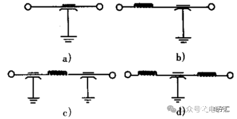
Figure 7 Types of Filters
3. Shielding. Due to space constraints and the abundance of articles discussing shielding, we will not elaborate further.
4. Try to reduce the speed of high-frequency devices.
5. Increase the dielectric constant of the PCB to prevent high-frequency components, such as transmission lines close to the board, from radiating outward; increase the thickness of the PCB to minimize the thickness of microstrip lines, which can prevent electromagnetic lines from leaking out and also prevent radiation.
In conclusion, we can summarize the principles we should follow in high-frequency PCB design:
1. Unified and stable power and ground.
2. Careful routing and appropriate termination can eliminate reflections.
3. Careful routing and appropriate termination can reduce capacitive and inductive crosstalk.
4. Noise suppression is required to meet EMC requirements.
 |
Sharing technical articles, news, and communication meetings related to electronics Subtle progress every day Gathering electronic technology |